ISL8499 Просмотр технического описания (PDF) - Renesas Electronics
Номер в каталоге
Компоненты Описание
Список матч
ISL8499
Renesas Electronics

ISL8499 Datasheet PDF : 14 Pages
| |||
ISL8499
approach, but the switch signal range is reduced and the
resistance may increase, especially at low supply voltages.
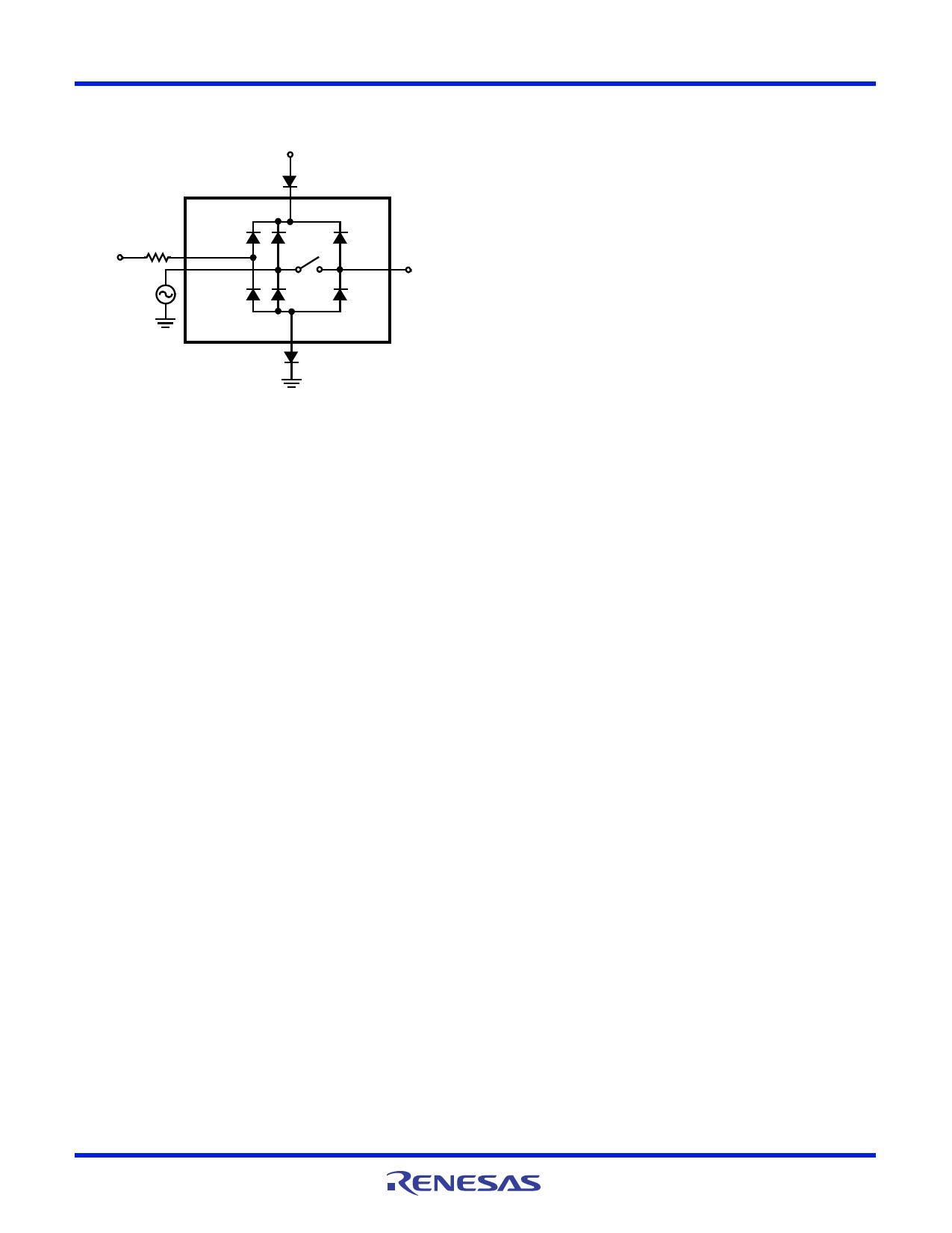
OPTIONAL
PROTECTION
RESISTOR
INX
VNO or NC
OPTIONAL PROTECTION
DIODE
V+
VCOM
GND
OPTIONAL PROTECTION
DIODE
FIGURE 8. OVERVOLTAGE PROTECTION
Power-Supply Considerations
The ISL8499 construction is typical of most single supply
CMOS analog switches, in that they have two supply pins: V+
and GND. V+ and GND drive the internal CMOS switches and
set their analog voltage limits. Unlike switches with a 4V
maximum supply voltage, the ISL8499 4.7V maximum supply
voltage provides plenty of room for the 10% tolerance of 4.3V
supplies, as well as room for overshoot and noise spikes.
The minimum recommended supply voltage is 1.65V but will
operate with a supply voltage below 1.5V. It is important to note
that the input signal range, switching times, and on-resistance
degrade at lower supply voltages. Refer to the “Electrical
Specification” tables starting on page 3 and “Typical
Performance” curves starting on page 6 for details.
V+ and GND also power the internal logic and level shiftiers.
The level shiftiers convert the input logic levels to switched V+
and GND signals to drive the analog switch gate terminals.
This family of switches cannot be operated with bipolar
supplies, because the input switching point becomes negative
in this configuration.
Logic-Level Thresholds
This switch family is 1.8V CMOS compatible (0.5V and 1.4V)
over a supply range of 2.7V to 4.5V (see Figure 14). At 2.7V
the VIL level is about 0.52V. This is still above the 1.8V CMOS
guaranteed low output maximum level of 0.5V, but noise
margin is reduced.
The digital input stages draw supply current whenever the
digital input voltage is not at one of the supply rails. Driving the
digital input signals from GND to V+ with a fast transition time
minimizes power dissipation. The ISL8499 has been designed
to minimize the supply current whenever the digital input
voltage is not driven to the supply rails (0V to V+). For example
driving the device with 2.85V logic (0V to 2.85V) while
operating with a 4.2V supply the device draws only 6A of
current (see Figure 21 for VIN = 2.85V).
High-Frequency Performance
In 50 systems, the signal response is reasonably flat even
past 30MHz with a -3dB bandwidth of 104MHz (see Figure 17).
The frequency response is very consistent over a wide V+
range, and for varying analog signal levels.
An OFF switch acts like a capacitor and passes higher
frequencies with less attenuation, resulting in signal
feedthrough from a switch’s input to its output. Off Isolation is
the resistance to this feedthrough, while Crosstalk indicates the
amount of feedthrough from one switch to another. Figure 18
details the high Off Isolation and Crosstalk rejection provided
by this part. At 100kHz, Off Isolation is about 68dB in 50
systems, decreasing approximately 20dB per decade as
frequency increases. Higher load impedances decrease Off
Isolation and Crosstalk rejection due to the voltage divider
action of the switch OFF impedance and the load impedance.
Leakage Considerations
Reverse ESD protection diodes are internally connected between
each analog-signal pin and both V+ and GND. One of these
diodes conducts if any analog signal exceeds V+ or GND.
Virtually all the analog leakage current comes from the ESD
diodes to V+ or GND. Although the ESD diodes on a given
signal pin are identical and therefore fairly well balanced, they
are reverse biased differently. Each is biased by either V+ or
GND and the analog signal. This means their leakages will
vary as the signal varies. The difference in the two diode
leakages to the V+ and GND pins constitutes the analog-
signal-path leakage current. All analog leakage current flows
between each pin and one of the supply terminals, not to the
other switch terminal. This is why both sides of a given switch
can show leakage currents of the same or opposite polarity.
There is no connection between the analog signal paths and
V+ or GND.
FN6111 Rev 3.00
February 5, 2008
Page 8 of 14
Share Link: