ISL84581 Просмотр технического описания (PDF) - Renesas Electronics
Номер в каталоге
Компоненты Описание
Список матч
ISL84581 Datasheet PDF : 15 Pages
| |||
ISL84581
Electrical Specifications 3.3V SupplyTest Conditions: V+ = +3.0V to +3.6V, V- = GND = 0V, VINH = 2.4V, VINL = 0.8V (Note 3),
Unless Otherwise Specified (Continued)
PARAMETER
TEST CONDITIONS
TEMP
MIN
MAX
(°C) (Notes 4, 8) TYP (Notes 4, 8) UNITS
INHIBIT Turn-OFF Time, tOFF
V+ = 3.0V, VNO = 1.5V, RL = 300, CL = 35pF,
25
-
37
50
ns
VIN = 0V to 3V (see Figure 1, Note 9)
Full
-
-
60
ns
Address Transition Time, tTRANS
V+ = 3.0V, VNO = 1.5V, RL = 300, CL = 35pF,
25
-
96
120
ns
VIN = 0V to 3V (see Figure 1, Note 9)
Full
-
-
145
ns
Break-Before-Make Time, tBBM
V+ = 3.6V, VNO = 1.5V, RL = 300, CL = 35pF,
Full
3
13
-
ns
VIN = 0V to 3V (see Figure 3, Note 9)
Charge Injection, Q
CL = 1.0nF, VG = 0V, RG = 0see Figure 2, Note 9) 25
-
0.3
1
pC
OFF-Isolation
RL = 50, CL = 15pF, f = 100kHz,
VNO = 1VRMS (see Figures 4 and 18)
25
-
92
-
dB
POWER SUPPLY CHARACTERISTICS
Power Supply Range
(Note 10)
Full
2
-
12
V
NOTES:
3. VIN = Input logic voltage to configure the device in a given state.
4. The algebraic convention, whereby the most negative value is a minimum and the most positive a maximum, is used in this data sheet.
5. rON = rON (MAX) - rON (MIN).
6. Flatness is defined as the difference between maximum and minimum value of on-resistance over the specified analog signal range.
7. Leakage parameter is 100% tested at high temp, and guaranteed by correlation at +25°C.
8. Parameters with MIN and/or MAX limits are 100% tested at +25°C, unless otherwise specified. Temperature limits established by characterization
and are not production tested.
9. Limits established by characterization and are not production tested.
10. Limits should be considered typical and are not production tested.
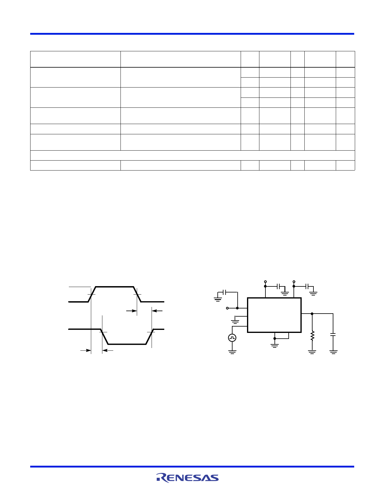
Test Circuits and Waveforms
3V
LOGIC
INPUT
0V
VNO0
SWITCH
OUTPUT 0V
tOFF
50%
tON
90% VOUT
tr < 20ns
tf < 20ns
90%
C
V+
LOGIC
INPUT
V+
C
V-
C
NO0
NO1-NO7
COM
INH
GND ADDA-C
VOUT
RL
300
CL
35pF
Logic input waveform is inverted for switches that have the opposite
logic sense.
FIGURE 1A. INHIBIT tON/tOFF MEASUREMENT POINTS
Repeat test for other switches. CL includes fixture and stray
capacitance.
VOUT = V(NO or NC) -R----L----R-+----Lr---O----N--
FIGURE 1B. INHIBIT tON/tOFF TEST CIRCUIT
FN6416 Rev 3.00
April 13, 2009
Page 7 of 15
Share Link: 