ML9092-03 Просмотр технического описания (PDF) - LAPIS Semiconductor Co., Ltd.
Номер в каталоге
Компоненты Описание
Список матч
ML9092-03 Datasheet PDF : 66 Pages
| |||
LAPIS Semiconductor
FEDL9092-01
ML9092-01/02/03/04
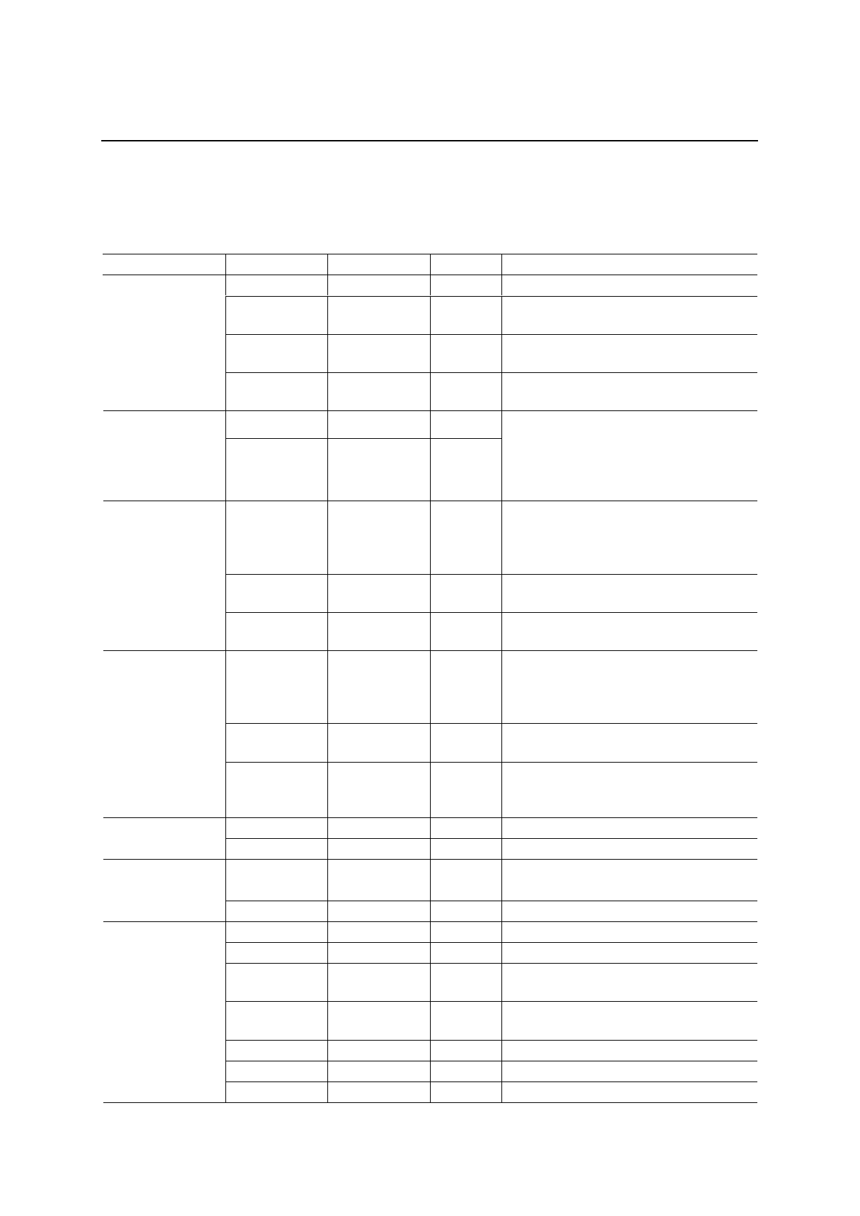
FUNCTIONAL DESCRIPTIONS
Pin Functional Descriptions
ML9092-01
Function
Pin
63
64
CPU interface
65
Symbol
CS
CP
DI/O
Oscillation
66
KREQ
77
OSC1
78
OSC2
Type
I
I
I/O
O
I
O
Control signal
67
RESET
I
80
KPS
I
79
TEST
I
Switch signal
Port output
LCD driver output
Power supply
62–58
C0/D0–C4/D4
I/O
57–53
R0/C0–R4/C4
O
51, 52
81
84–82
50–1
100–95
94–85
76
68
75
74, 73
72
71, 69
70
A, B
I
PA0
O
PB0–PB2
O
SEG1–SEG56
O
COM1–COM10
O
VDD
—
VSS
—
VIN
—
VC1+, VS1–
—
VOUT
—
V0, V2
—
NC
—
Description
Chip select signal input pin
Shift clock signal input pin. This pin is
connected to the Schmitt circuit internally.
Serial data signal I/O pin. This pin is
connected to the Schmitt circuit internally.
Key scan read and rotary encoder read
READY signal output pin.
Connect external resistors with this pin.
This pin is connected to the Schmitt circuit
internally.
If using an external clock, input it from the
OSC1 pin and leave the OSC2 pin open.
Reset input. Initial settings can be
established by applying a “L” level to this
pin. This pin is connected to the Schmitt
circuit internally.
Input pin for switching between key
scanning and ports C and D
Test input pin. This pin is connected to the
VSS pin.
Input pins that detect status of key
switches/port D output pins. When used
as input pins, these pins are connected to
the Schmitt circuit internally.
Key switch scan signal output pins/port C
output pins
Rotary encoder signal input pins.
These pins are connected to the Schmitt
circuit internally.
Port A output pin
Port B output pins
LCD segment driver output pins
LCD common driver output pins
Logic power supply pin
GND pin
Voltage doubler reference voltage input
pin
Pins to connect a capacitor for voltage
doubler
Voltage doubler output pin
LCD bias pins
Should be left open.
11/66
Share Link: 