PI74AVC16836AE Просмотр технического описания (PDF) - Pericom Semiconductor Corporation
Номер в каталоге
Компоненты Описание
Список матч
PI74AVC16836AE
Pericom Semiconductor Corporation

PI74AVC16836AE Datasheet PDF : 10 Pages
| |||
PI74AVC+16836 111222333444555666777888999000111222333444555666777888999000111222333444555666777888999000111222111222333444555666777888999000111222333444555666777888999000111222333444555666777888999000111222111222333444555666777888999000111222333444555666777888999000111222333444555666777888999000111222111222333444555666777888999000111222333444555666777888999000111222333444555666777888999000111222111222333444555
2.5V 20-Bit Universal Bus
Driver with 3-State Outputs
Features
• PI74AVC+16836 is designed for low-voltage operation,
VCC = 1.65V to 3.6V
• True ±24mA Balanced Drive @ 3.3V
• IOFF supports partial power-down operation
• 3.6V I/O Tolerant inputs and outputs
• Meets PC133 SDRAM Registered DIMM Specifications
• All outputs contain a patented DDC
(Dynamic Drive Control) circuit that reduces noise without
degrading propagation delay
• Industrial operation: –40°C to +85°C
• Packaging (Pb-free & Green available):
– 56-pin 240-mil wide plastic TSSOP (A)
Description
Pericom Semiconductor’s 20-bit PI74AVC+16836 universal bus
driver is designed for 1.65V to 3.6V VCC operation.
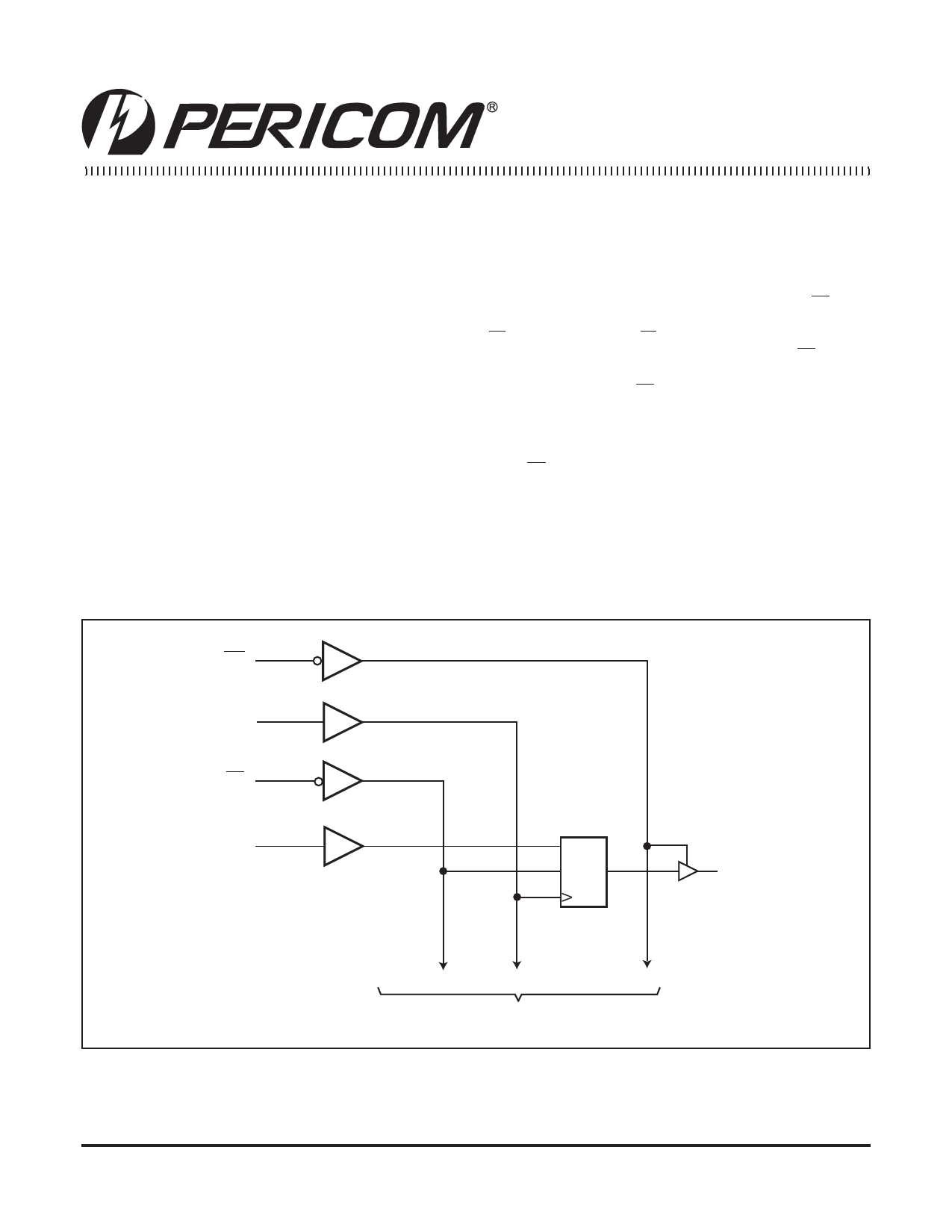
Data flow from A to Y is controlled by the Output Enable (OE) input.
The device operates in the transparent mode when the latch-enable
(LE) input is LOW. When LE is HIGH, the A data is latched if the
clock (CLK) input is held at a high or low logic level. If LE is HIGH,
the A data is stored in the latch/flip-flop on the low-to-high
transition of CLK. When OE is HIGH, the outputs are in the high-
impedance state, but all the inputs are enabled and data is capable
of being stored in the register.
To ensure the high-impedance state during power up or power
down, OE should be tied to VCC through a pullup resistor; the
minimum value of the resistor is determined by the current-sinking
capability of the driver.
Block Diagram
1
OE
56
CLK
29
LE
A1 55
1D
C1
CLK
2
Y1
TO 19 OTHER CHANNELS
08-0291
1
PS8511E 10/17/08
Share Link: