MB88151A-401 Просмотр технического описания (PDF) - Unspecified
Номер в каталоге
Компоненты Описание
Список матч
MB88151A-401 Datasheet PDF : 4 Pages
| |||
The Fujitsu SSCG
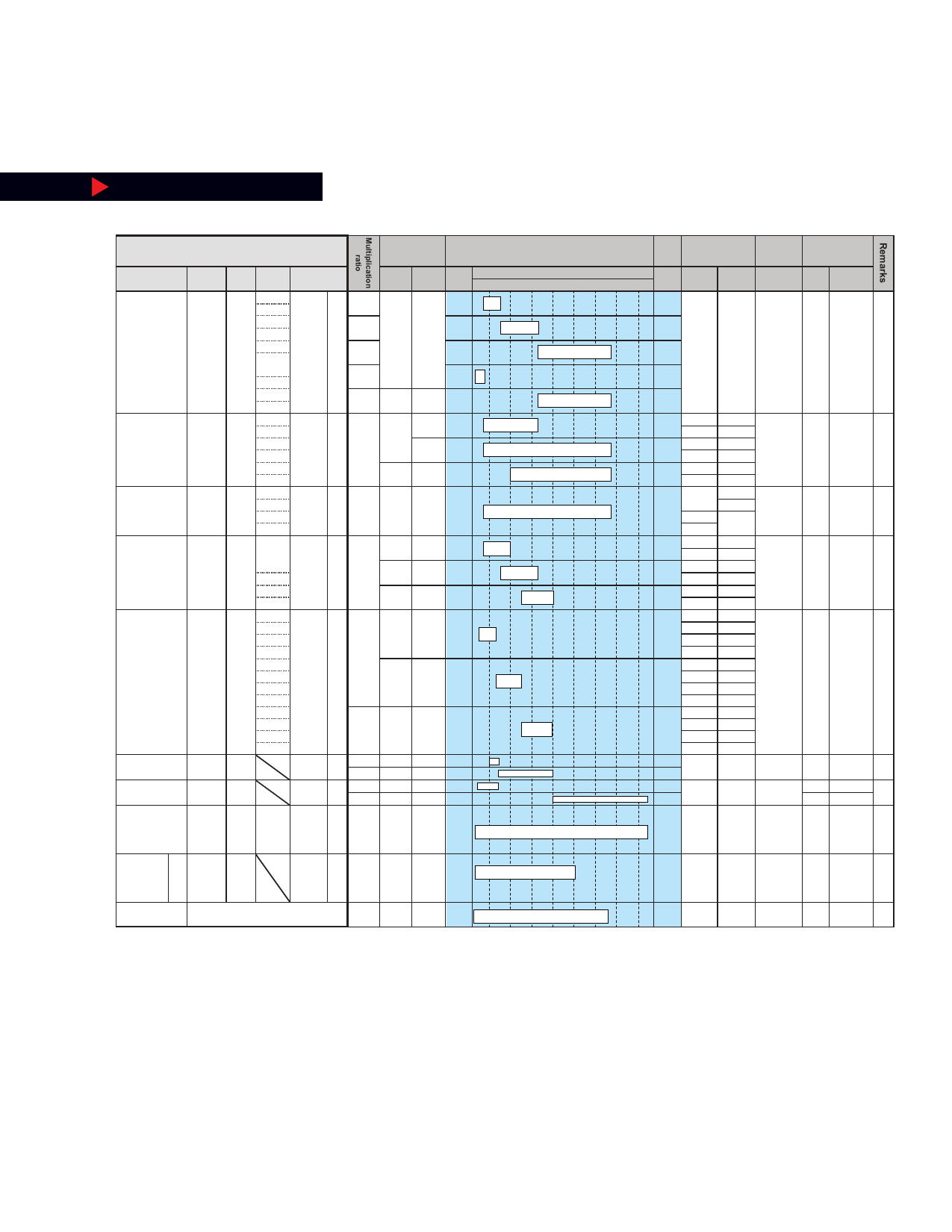
Parts Ordering Information
ORDERING No.
EX: MB881XXPNF-G-100-JNE1
Product No.
MB88151A
MB88152A
MB88153A
MB88154A
MB88155
MB88161
MB88162
Pakage Grade Freq Packing and
Suffix (*1) type Option(*2)
100
1
101
200
2
PNF
G
201
400
JN/
JNEF/ E1
401 JNER
4
500
501
1/2
800
8
801
101
PNF
G
111
100
110
JN/
JNEF/ E1
JNER
1
102
112
PNF
G
100
101
110
JN/
JNEF/ E1
JNER
1
111
103
PNF
G
113
102
JN/
JNEF/ E1
1
112 JNER
101
111
100
110
102
112
1
101
PFT G 111 JN E1
103
113
400
402
410
4
412
PVB G
EF/
ER
E1
1
2
PVB G
EF/
ER
E1
1
4
Input
frequency
(MHz)
Min. max. Min.
16.6
33.2
16.6 33.4
66.4
8.3
8.3 16.7 66.4
67 16.6
16.6
134 16.6
40 134 40
16.6 134 16.6
16.6 40 16.6
33 67 33
50 80 50
12.5 25 12.5
25 50 25
12.5 20 50
20 28 20
14 40 28
12 28 12
20 42 80
Output frequency (MHz)
Output frequency range
40ᇫᇫᇫ80ᇫᇫᇫ120 ᇫ160
Demodulation
rate(%)
PKG
P/S(V)
Max. Center
Down
No. of
pins/Type
Min.
Max.
33.4
66.8
134 ᨺ±1.5 ᨺ3.0
8
SOP
3.0
3.6
16.7
134
67
᧩
ᨺ3.0
ᨺ±1.5 ᧩
134
᧩
ᨺ±1.5
ᨺ3.0
᧩
8
SOP
3.0
3.6
134
᧩
ᨺ±1.5
ᨺ3.0
᧩
᧩
-1.0
134
-3.0
±0.5
᧩
±1.5
8
SOP
3.0
3.6
*4
40
᧩
ᨺ3.0
ᨺ±1.5 ᧩
67
᧩
ᨺ3.0
ᨺ±1.5 ᧩
8
SOP
3.0
3.6
80
᧩
ᨺ±1.5
ᨺ3.0
᧩
᧩ ᨺ2.0
25 ᨺ±1.0
᧩
᧩ ᨺ2.0
ᨺ±1.0 ᧩
᧩ ᨺ2.0
50
ᨺ±1.0 ᧩
᧩ ᨺ2.0
8
TSSOP
3.0
3.6
ᨺ±1.0 ᧩
᧩ ᨺ2.0
80
᧩
ᨺ2.0
ᨺ±1.0 ᧩
ᨺ±1.0 ᧩
28
80 ᨺ±2.0 ᨺ4.0
18
BCC
2.7
3.6
*5
28
168 ᨺ±2.0 ᨺ4.0
18
2.7
BCC 3.0
3.6
3.6
*5
MB88181A
PFT
G XXX BND E1 Option- 16
al
32
8
20
166 ᨺ±2.0 ᧩
TSSOP 3.0
3.6
*7
1A
MB88182
1B
2A
PVA1
G
2B
(*3)/
ER/
E1
Option-
al
19.2
19.2
8
EF
100 ᨺ±2.0 ᧩ 20 BCC 1.65 2.7 *8
MB88R157
(FRAM)
under development
Option-
al
10
50
1
134 ᨺ±1.75 ᧩ 8 SOP 3.0 3.6 *9
*1 G: General Purpose use
*2 JN: tray or tube packing , JNEF/EF: Emboss taping(EF type), JNER/ER: Emboss taping(ER type), E1: Lead free
*3 No suffix : tray or tube packing
*4 Use for external clock input
*5 Small package (2.7mm×2.4mm) with clock output stop function
*6 Small package (2.4mm×1.4mm)
*7 Multiplication ratio and output frequency are the MASK option.CLK output has eight pins. The output pin state during power-down is fixed by mask option.᧤L outputsᇬHi-Z᧥
*8 Input frequency, output frequency, modulation rate, oscillation stabilization, capacitance can be set. The output pin state during power-down is fixed by mask option (L outputs,Hi-Z᧥
*9 Input frequency, output frequency, modulation rate, oscillation stabilization capacitance can be set on FRAM without restraint.
Modulation clock output pin situation is resistor setting᧤L outputs,Hi-Z᧥when in OE pin setting
Share Link: 