SPX3940T-L-3-3 Просмотр технического описания (PDF) - Exar Corporation
Номер в каталоге
Компоненты Описание
Список матч
SPX3940T-L-3-3 Datasheet PDF : 11 Pages
| |||
SPX3 9 4 0
1 A Low Dr opou t Volt age Regu lat or
ABSOLUTE MAXIMUM RAT INGS
These are stress ratings only and functional operation of
the device at these ratings or any other above those
indicated in the operation sections of the specification
s
below is not implied. Exposure to absolute maximum
rating conditions for extended periods of time may affect
reliability.
Input Voltage V IN ................................
................... 20 V1
Storage Temperature ..............................
- 65°C to 150°C
Lead Temperature (Soldering, 5 sec) ..................... 26 0°C
OPERATING RATINGS
Input Voltage VIN ................................
.................... 16V
Junction Temperature Range .................... - 40°C to 1 25 °C
Package s Thermal Resistance
SOT- 223 Junction to Case (at T A) ..................... 15 °C/W
SOT- 223 Junction to Ambient ........................ 62.3°C/W
TO- 263 Junction to Case (at T A) ......................... 3°C/W
TO- 263 Junction to Ambient .......................... 31.4 °C/W
Note 1: Maximum positive supply voltage of 20V must be
of limited duration (<100ms) and duty cycle (<1%). The
maximum continuous supply voltage is 16V.
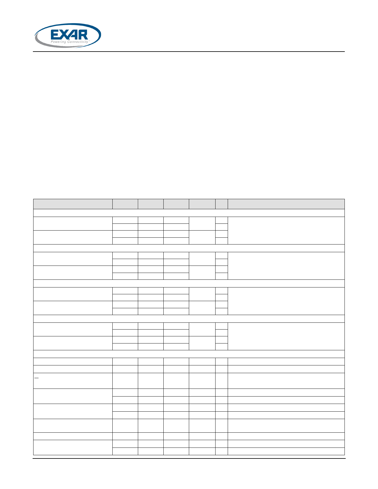
ELECTRICAL SPECIFICA TIONS
Specifications with standard type are for
an Operating Ambient Temperature of TA = 25°C only; limits a pplying over the full
2SHUDWLQJ -XQFWLRQ 7HPSHUDWXUH´UDQ0JLHQLDPUXHPGDHQQGRW0HDG[LEP\XPDO³LPLWV DUH JXDUD
design, or statistical correlation. Typical values represent the most likely parametric norm at T
A = 25°C, and are prov ided
for reference purposes only. Unless otherwise indicated, V
IN = VIN +1V , I OUT = 10mA, CIN = 6.8 µF, COUT = 10 µF, TA = 25°C .
Parameter
1.8V version
Output Voltage - SPX3940A (1%)
Output Voltage - SPX3940 (2%)
2.5V version
Output Voltage - SPX3940A (1%)
Output Voltag e - SPX3940 (2%)
3.3V version
Output Voltage - SPX3940A (1%)
Output Voltage - SPX3940 (2%)
5 .0 V version
Output Voltage - SPX3940A (1%)
Output Voltage - SPX3940 (2%)
All Voltage Options
Line Regulation
Load Regulation
ο - Output Voltage
ο்
temperature Coefficient
Dropout Voltage 2
(except 1.8V version)
Ground Current 3
I GNDDO Ground Pin Current at
Dropout
Current Limit
Output Noise Voltage
Min.
1.782
1.755
1.764
1.737
2.475
2.437
2.450
2.412
3.267
3.217
3.234
3.184
4.950
4.875
4.900
4.825
1.5
Typ.
1.8
1.8
1.8
1.8
2.5
2.5
2.5
2.5
3.3
3.3
3.3
3.3
5.0
5.0
5.0
5.0
0.2
0.3
20
70
280
12
18
1.2
2.2
400
26 0
Max.
Units
Conditions
1.818
1.845
1.836
1.863
V
I OUT=10mA
V
P$OU,T$IN999
2.525
2.563
2.550
2.588
V
I OUT=10mA
V
P$OU,T$IN999
3.333
3.383
3.366
3.416
V
I OUT=10mA
V
P$OU,T$IN999
5.050
5.125
5.100
5.175
V
I OUT=10mA
V
P$OU,T$IN999
1.0
%
1.5
%
I OUT=10mA, (V OUT 9
IN 99
VIN = V OUT 9PO$UT,$
100
ppm/°C
200
mV
I OUT=100mA
550
mV
I OUT=1A
25
mA
I OUT=750mA, V IN = V OUT +1V
mA
I OUT=1A
mA
A
µV RMS
µV RMS
VIN = 0.1V less than specified V OUT I OUT=10mA,
VOUT = 0V 4
10Hz - 100KHz, I L=100mA, C L=10µF
10Hz - 100KHz, I L=100mA, C L=33µF
© 2012 Exar Corporation
2/ 11
Rev. 1.0.0
Share Link: 