CS8121 Просмотр технического описания (PDF) - ON Semiconductor
Номер в каталоге
Компоненты Описание
Список матч
CS8121 Datasheet PDF : 8 Pages
| |||
Application Notes: continued
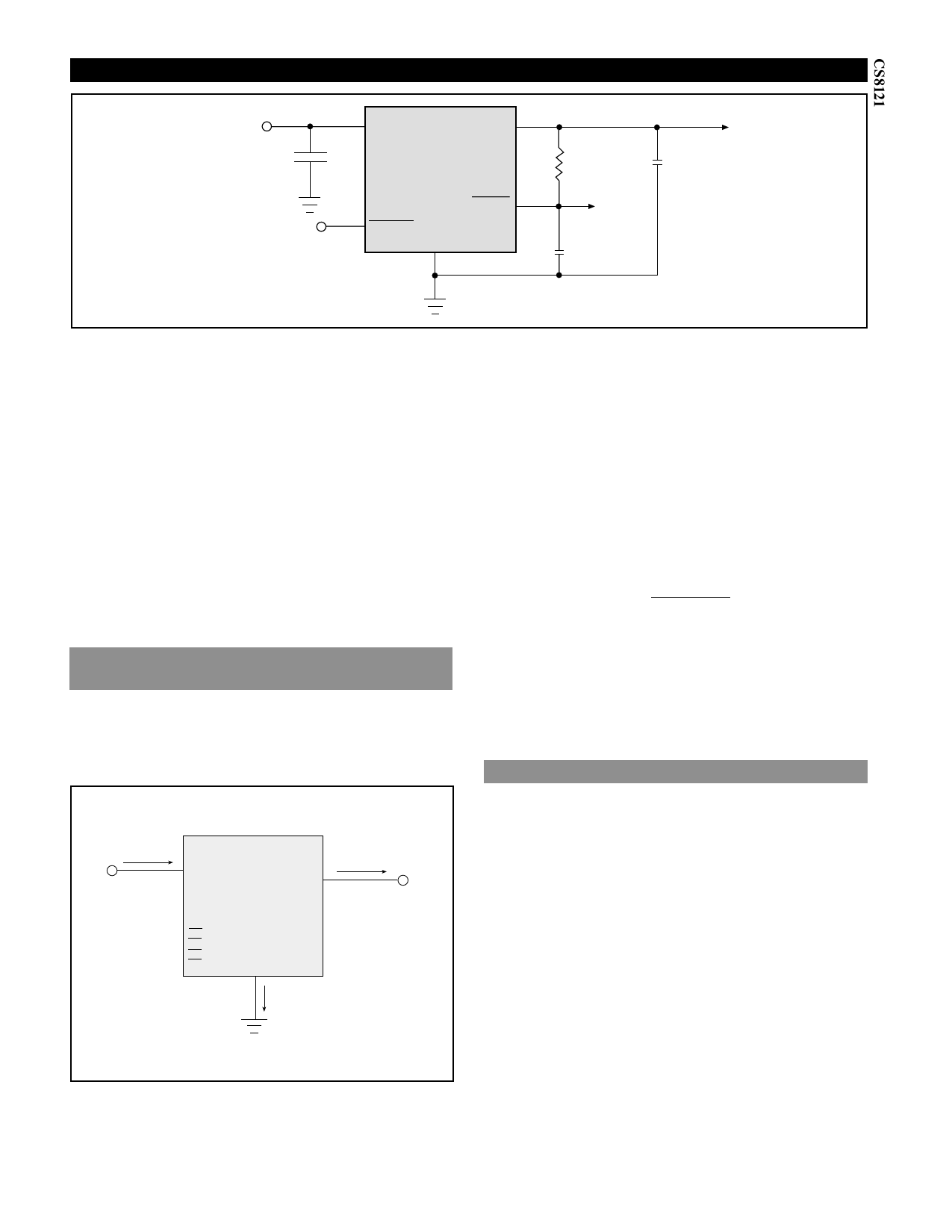
VIN
C1*
0.1µF
C1*required if regulator is located far from
the power supply filter.
C2** required for stability.
VOUT
CS8121
ENABLE
RESET
RRST
to µP
RESET
Port
CRST
C2**
10µF
5V to µP and
System
Power
Figure 6: Test and application circuit showing output compensation.
Step 6: Test the load transient response by switching in
various loads at several frequencies to simulate its real
working environment. Vary the ESR to reduce ringing.
Step 7: Remove the unit from the environmental chamber
and heat the IC with a heat gun. Vary the load current as
instructed in step 5 to test for any oscillations.
Once the minimum capacitor value with the maximum
ESR is found, a safety factor should be added to allow for
the tolerance of the capacitor and any variations in regula-
tor performance. Most good quality aluminum electrolytic
capacitors have a tolerance of +/- 20% so the minimum
value found should be increased by at least 50% to allow
for this tolerance plus the variation which will occur at
low temperatures. The ESR of the capacitor should be less
than 50% of the maximum allowable ESR found in step 3
above.
Calculating Power Dissipation
in a Single Output Linear Regulator
The maximum power dissipation for a single output regu-
lator (Figure 7) is:
PD(max) = {VIN(max) - VOUT(min)}IOUT(max) + VIN(max)IQ
(1)
IIN
VIN
Smart
Regulator
}Control
Features
IQ
IOUT
VOUT
Figure 7: Single output regulator with key performance parameters
labeled.
where:
VIN(max) is the maximum input voltage,
VOUT(min) is the minimum output voltage,
IOUT(max) is the maximum output current for the applica-
tion, and
IQ is the quiescent current the regulator consumes at
IOUT(max).
Once the value of PD(max) is known, the maximum permis-
sible value of RΘJA can be calculated:
RΘJA =
150°C - TA
PD
(2)
The value of RΘJA can then be compared with those in
the package section of the data sheet. Those packages
with RΘJA's less than the calculated value in equation 2
will keep the die temperature below 150°C.
In some cases, none of the packages will be sufficient to
dissipate the heat generated by the IC, and an external
heatsink will be required.
Heat Sinks
A heat sink effectively increases the surface area of the
package to improve the flow of heat away from the IC
and into the surrounding air.
Each material in the heat flow path between the IC and
the outside environment will have a thermal resistance.
Like series electrical resistances, these resistances are
summed to determine the value of RΘJA:
RΘJA = RΘJC + RΘCS + RΘSA
(3)
where:
RΘJC = the junction–to–case thermal resistance,
RΘCS = the case–to–heatsink thermal resistance, and
RΘSA = the heatsink–to–ambient thermal resistance.
RΘJC appears in the package section of the data sheet. Like
RΘJA, it too is a function of package type. RΘCS and RΘSA
are functions of the package type, heatsink and the inter-
face between them. These values appear in heat sink data
sheets of heat sink manufacturers.
7
Share Link: 