IN74HC573A Просмотр технического описания (PDF) - IK Semicon Co., Ltd
Номер в каталоге
Компоненты Описание
Список матч
IN74HC573A Datasheet PDF : 6 Pages
| |||
IN74HC573A
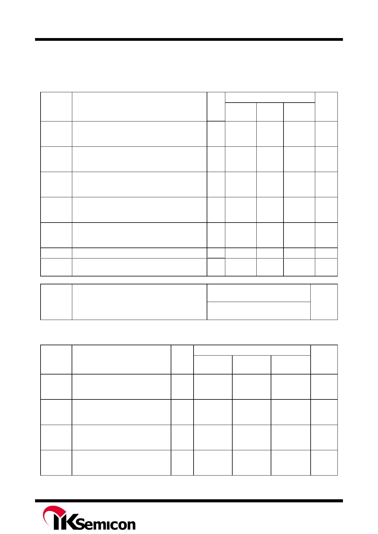
AC ELECTRICAL CHARACTERISTICS(CL=50pF,Input tr=tf=6.0 ns)
Symbol
Parameter
tPLH, tPHL Maximum Propagation Delay, Input D to Q
(Figures 1 and 5)
tPLH, tPHL Maximum Propagation Delay, LE to Q
(Figures 2 and 5)
tPLZ, tPHZ Maximum Propagation Delay, OE to Q
(Figures 3 and 6)
tPZH, tPZL Maximum Propagation Delay, OE to Q
(Figures 3 and 6)
tTLH, tTHL Maximum Output Transition Time, Any Output
(Figures 1 and 5)
CIN
COUT
Maximum Input Capacitance
Maximum Three-State Output Capacitance
(Output in High-Impedance State)
VCC
Guaranteed Limit
V 25 °C to ≤85°C ≤125°C Unit
-55°C
2.0 150
190
225
ns
4.5
30
38
45
6.0
26
33
38
2.0 160
200
240
ns
4.5
32
40
48
6.0
27
34
41
2.0 150
190
225
ns
4.5
30
38
45
6.0
26
33
38
2.0 150
190
225
ns
4.5
30
38
45
6.0
26
33
38
2.0
60
75
90
ns
4.5
12
15
18
6.0
10
13
15
-
10
10
10
pF
-
15
15
15
pF
Power Dissipation Capacitance (Per Enabled
Output)
CPD Used to determine the no-load dynamic power
consumption: PD=CPDVCC2f+ICCVCC
Typical @25°C,VCC=5.0 V
23
pF
TIMING REQUIREMENTS (CL=50pF,Input tr=tf=6.0 ns)
Symbol
Parameter
VCC
Guaranteed Limit
V
25 °C to
-55°C
≤85°C
≤125°C
Unit
tSU Minimum Setup Time, Input D to
2.0
50
65
75
ns
Latch Enable
4.5
10
13
15
(Figure 4)
6.0
9
11
13
th
Minimum Hold Time, Latch Enable 2.0
5
5
5
ns
to Input D
4.5
5
5
5
(Figure 4)
6.0
5
5
5
tw
Minimum Pulse Width, Latch
2.0
75
95
110
ns
Enable (Figure 2)
4.5
15
19
22
6.0
13
16
19
tr, tf Maximum Input Rise and Fall
Times (Figure 1)
2.0
1000
4.5
500
6.0
400
1000
500
400
1000
ns
500
400
Rev. 00
Share Link: 