MK1725 Просмотр технического описания (PDF) - Integrated Device Technology
Номер в каталоге
Компоненты Описание
Список матч
MK1725 Datasheet PDF : 8 Pages
| |||
MK1725
QUAD OUTPUT SPREAD SPECTRUM CLOCK GENERATOR
SSCG
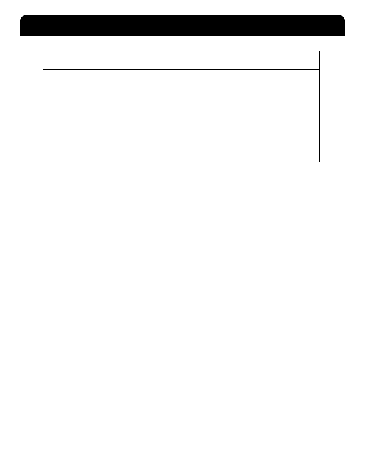
Pin
Number
10
11
12
13
14
15
16
Pin
Name
CLK4
GND
VDD
S2
PDTS
VDD
X2
Pin
Type
Pin Description
Output Clock 4 output. Frequency and spread amount are determined
by table above. Weak internal pull-down when tri-state.
Power Connect to ground.
Power Connect to +3.3 V.
Input Select pin 2. Determines frequency and spread amount on
output clocks as per table above. Internal pull-down.
Input
Power Down Tri-state. Powers down entire chip and tri-states
outputs when low. Internal pull-up resistor.
Power Connect to +3.3V.
Input 20 MHz to 34 MHz crystal input. Float for clock input.
External Components
Decoupling Capacitor
As with any high performance mixed-signal IC, the MK1725
must be isolated from system power supply noise to perform
optimally.
A decoupling capacitor of 0.01µF must be connected
between each VDD and the PCB ground plane.
Series Termination Resistor
Clock output traces over one inch should use series
termination. To series terminate a 50Ω trace (a commonly
used trace impedance), place a 33Ω resistor in series with
the clock line, as close to the clock output pin as possible.
The nominal impedance of the clock output is 20Ω.
Crystal Load Capacitors
The device crystal connections should include pads for
small capacitors from X1 to ground and from X2 to ground.
These capacitors are used to adjust the stray capacitance of
the board to match the nominally required crystal load
capacitance. Because load capacitance can only be
increased in this trimming process, it is important to keep
stray capacitance to a minimum by using very short PCB
traces (and no vias) between the crystal and device. Crystal
capacitors must be connected from each of the pins X1 and
X2 to ground.
PCB Layout Recommendations
For optimum device performance and lowest output phase
noise, the following guidelines should be observed.
1) The 0.01µF decoupling capacitors should be mounted on
the component side of the board as close to the VDD pin as
possible. No vias should be used between the decoupling
capacitors and VDD pins. The PCB trace to VDD pins
should be kept as short as possible, as should the PCB
trace to the ground via.
2) The external crystal should be mounted just next to the
device with short traces. The X1 and X2 traces should not
be routed next to each other with minimum spaces, instead
they should be separated and away from other traces.
3) To minimize EMI the 33Ω series termination resistor (if
needed) should be placed close to the clock outputs.
4) An optimum layout is one with all components on the
same side of the board, minimizing vias through other signal
layers. Other signal traces should be routed away from the
MK1725. This includes signal traces just underneath the
device, or on layers adjacent to the ground plane layer used
by the device.
The value (in pF) of these crystal caps should equal (CL
-6)*2. In this equation, CL= crystal load capacitance in pF.
Example: For a crystal with an 18 pF load capacitance, each
crystal capacitor would be 24 pF [(18-6) x 2 = 24].
IDT™ QUAD OUTPUT SPREAD SPECTRUM CLOCK GENERATOR
3
MK1725
REV G 033109
Share Link: 