MAX186ACAP Просмотр технического описания (PDF) - Maxim Integrated
Номер в каталоге
Компоненты Описание
Список матч
MAX186ACAP Datasheet PDF : 24 Pages
| |||
Low-Power, 8-Channel,
Serial 12-Bit ADCs
________________________________________________Pin Description (continued)
PIN
NAME
FUNCTION
Input to the Reference-Buffer Amplifier. To disable the reference-buffer amplifier, tie REFADJ to
12
REFADJ
VDD.
13
AGND
Analog Ground. Also IN- Input for single-ended conversions.
14
DGND
Digital Ground
15
DOUT
Serial Data Output. Data is clocked out at the falling edge of SCLK. High impedance when CS is high.
Serial Strobe Output. In internal clock mode, SSTRB goes low when the MAX186/MAX188 begin the
16
SSTRB
A/D conversion and goes high when the conversion is done. In external clock mode, SSTRB pulses
high for one clock period before the MSB decision. High impedance when CS is high (external mode).
17
DIN
Serial Data Input. Data is clocked in at the rising edge of SCLK.
18
CS
Active-Low Chip Select. Data will not be clocked into DIN unless CS is low. When CS is high, DOUT
is high impedance.
19
SCLK
Serial Clock Input. Clocks data in and out of serial interface. In external clock mode, SCLK also sets
the conversion speed. (Duty cycle must be 40% to 60% in external clock mode.)
20
VDD
Positive Supply Voltage, +5V ±5%
+5V
DOUT
3k
DOUT
3k
CLOAD
CLOAD
DGND
DGND
a. High-Z to VOH and VOL to VOH
b. High-Z to VOL and VOH to VOL
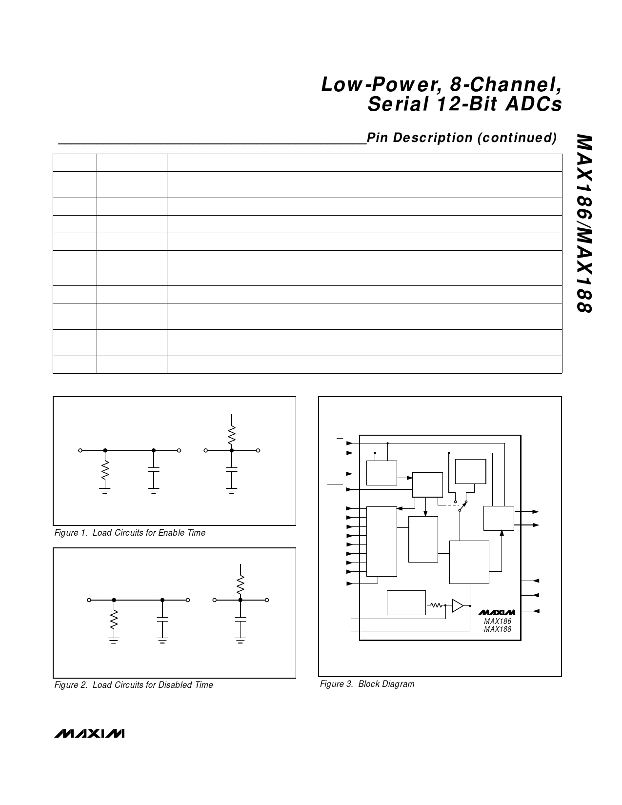
Figure 1. Load Circuits for Enable Time
DOUT
+5V
3k
DOUT
3k
DGND
CLOAD
CLOAD
DGND
a VOH to High-Z
b VOL to High-Z
Figure 2. Load Circuits for Disabled Time
CS 18
SCLK 19
DIN 17
SHDN 10
INPUT
SHIFT
REGISTER
CONTROL
LOGIC
INT
CLOCK
CH0 1
CH1 2
CH2 3
CH3 4
CH4 5
CH5 6
CH6 7
CH7 8
AGND 13
REFADJ 12
VREF 11
OUTPUT
SHIFT
REGISTER
ANALOG
INPUT
T/H
MUX
CLOCK
IN12-BIT
SAR
ADC OUT
REF
+2.46V
REFERENCE
A ≈ 1.65
20k
(MAX186)
+4.096V
MAX186
MAX188
15 DOUT
16 SSTRB
20 VDD
14 DGND
9
VSS
Figure 3. Block Diagram
_______________________________________________________________________________________ 7
Share Link: 