CMX631A Просмотр технического описания (PDF) - MX-COM Inc
Номер в каталоге
Компоненты Описание
Список матч
CMX631A Datasheet PDF : 12 Pages
| |||
Low Voltage SPM Detector
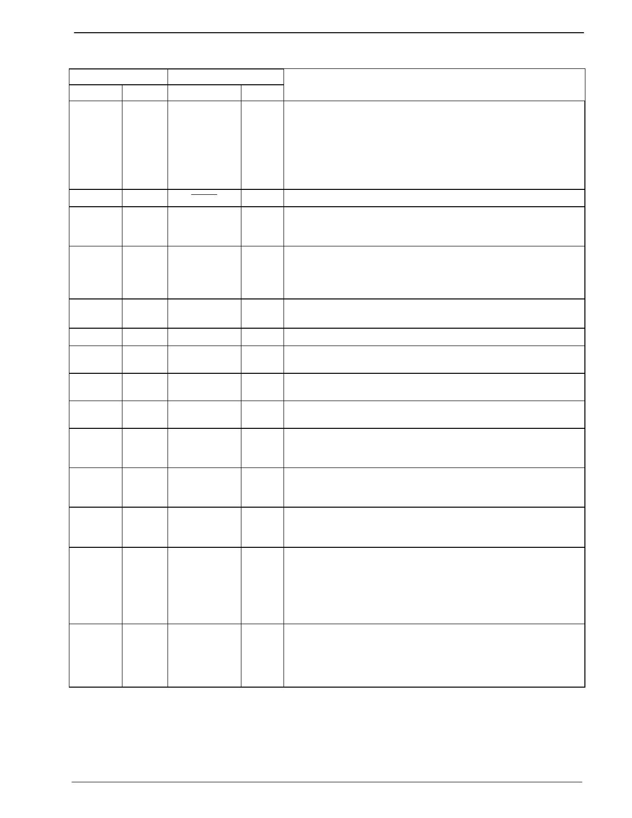
2 Signal List
4
CMX631A PRELIMINARY INFORMATION
Packages
D5
D4/P3
1
1
4
2
5
3
6
4
8
7
12
8
13
9
17
10
18
11
19
13
20
14
21
15
24
16
2, 3, 7,
9, 10,
11, 14,
15, 16,
22, 23
5,6,12
Signal
Name
Type
Xtal/Clock input
XTAL
Clock Out
output
output
Clock In
input
VBIAS
power
VSS
Signal In +
power
input
Signal In - input
Amp Out input
Tone
Follower
Mode
Packet Mode
output
output
System
input
VDD
power
N/C
Description
The input to the on-chip clock oscillator; for use with a
3.579545MHz Xtal in conjunction with the Xtal output; circuit
components are on-chip. When using a Xtal input, the Clock
Out pin should be connected directly to the Clock In pin. If a
clock pulse input is used at the Clock In pin, this (Xtal/Clock)
pin must be connected directly to VDD See Figure 2 and
Section 3.
The output of the on-chip clock oscillator inverter.
The buffered output of the on-chip-clock oscillator inverter. If a
Xtal input is used, this output should be connected directly to
the Clock In pin.
The 3.579545MHz clock pulse input to the internal clock
dividers. If an externally generated clock pulse is used, the
Xtal/Clock input pin should be connected to VDD. Reference
Section 3.
The output of the on-chip analog bias circuitry. Held internally
at VDD/2, this pin should be bypassed to VSS. See Figure 2.
Negative supply (GND).
The positive input to the input gain adjusting signal amplifier.
Reference Section 4.3 and 4.4.
The negative input to the input gain adjusting signal amplifier.
Reference Section 4.3 and 4.4.
The output of the input gain adjusting signal amplifier.
Reference Section 4.3 and 4.4.
This output provides a logic 0 for the period of a detected tone
and a logic 1 for a NOTONE detection. See Section 4.1 and
Figure 3.
This output provides a logic 0 for a detected tone and a logic 1
for NOTONE detection and will ignore a small fluctuation or
fade during the tone signal. See Section 4.2 and Figure 3.
This logic input selects the device operation to either 12kHz
(logic 1) or 16kHz (logic 0) SPM systems. This input has an
internal 1MΩ pull-up resistor (12kHz).
Positive supply. A single, stable power supply is required.
Critical levels and voltages within the CMX631A are dependent
upon this supply. This pin should be bypassed to VSS by a
capacitor mounted close to the pin. Note: If this device is line
powered, the resulting power supply must be stable. See
Section 5.1.1.
No internal connection; leave open circuit.
Table 1: Signal List
© 1999 MX•COM Inc.
www.mxcom.com Tele: 800 638-5577 336 744-5050 Fax: 336 744-5054
Doc. # 20480177.004
4800 Bethania Station Road, Winston-Salem, NC 27105-1201 USA All trademarks and service marks are held by their respective companies.
Share Link: 