NCP1547(2007) Просмотр технического описания (PDF) - ON Semiconductor
Номер в каталоге
Компоненты Описание
Список матч
NCP1547 Datasheet PDF : 13 Pages
| |||
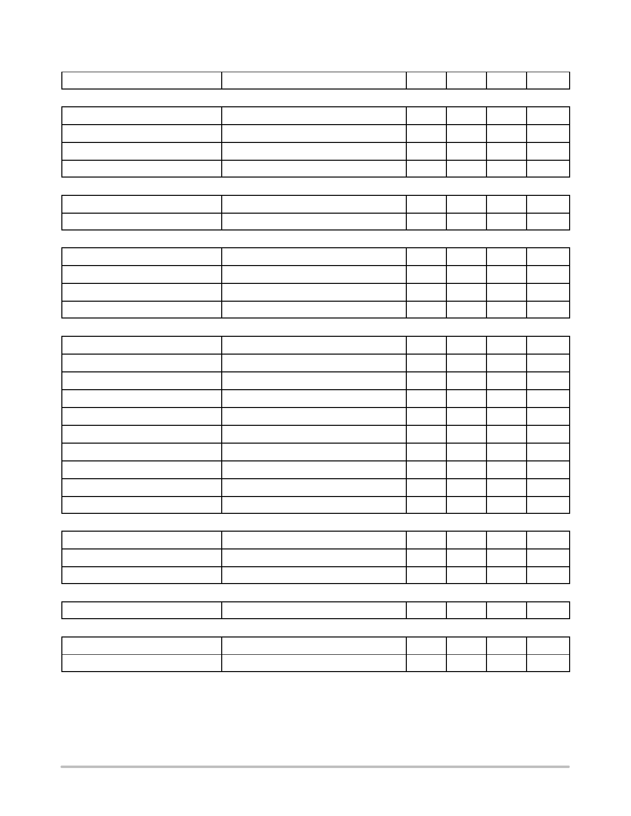
NCP1547
ELECTRICAL CHARACTERISTICS (0°C < TJ < 70°C, 4.5 V< VIN < 40 V; unless otherwise specified.)
Characteristic
Test Conditions
Min
Oscillator
Operating Frequency
−
306
Frequency Line Regulation
−
−
Maximum Duty Cycle
−
85
VFB Frequency Foldback Threshold
PWM Comparator
−
0.29
Slope Compensation Voltage
Fix VFB, DVC/DTON
5.0
Minimum Output Pulse Width
VFB to VSW
−
Power Switch
Current Limit
Foldback Current
Saturation Voltage
Current Limit Delay
VFB > 0.36 V
1.6
VFB < 0.29 V
0.9
IOUT = 1.5 A, VBOOST = VIN + 2.5 V
0.4
(Note 3)
−
Error Amplifier
Internal Reference Voltage
−
1.244
Reference PSRR
(Note 3)
−
FB Input Bias Current
−
−
Output Source Current
Output Sink Current
Output High Voltage
Output Low Voltage
Unity Gain Bandwidth
VC = 1.270 V, VFB = 1.0 V
VC = 1.270 V, VFB = 2.0 V
VFB = 1.0 V
VFB = 2.0 V
(Note 3)
15
15
1.39
5.0
−
Open Loop Amplifier Gain
(Note 3)
−
Amplifier Transconductance
(Note 3)
−
Sync
Sync Frequency Range
−
377
Sync Pin Bias Current
VSYNC = 5.0 V
−
Sync Threshold Voltage
−
0.9
Shutdown
Shutdown Threshold Voltage
−
1.0
Shutdown Pin Bias Current
Thermal Shutdown
VSHDNB = 0 V
0.14
Overtemperature Trip Point
(Note 3)
175
Thermal Shutdown Hysteresis
(Note 3)
−
3. Guaranteed by design, not 100% tested in production.
Typ
340
0.05
90
0.32
9.0
100
2.3
1.5
0.7
120
1.270
40
0.02
25
25
1.46
20
500
70
6.4
−
360
1.5
1.3
5.00
185
42
Max
374
0.15
95
0.36
17
200
3.0
2.1
1.0
160
1.296
−
0.1
35
35
1.53
60
−
−
−
710
485
1.9
1.6
35
195
−
Unit
kHz
%/V
%
V
mV/ms
ns
A
A
V
ns
V
dB
mA
mA
mA
V
mV
kHz
dB
mA/V
kHz
mA
V
V
mA
°C
°C
http://onsemi.com
4
Share Link: 