RT9182(2007) Просмотр технического описания (PDF) - Richtek Technology
Номер в каталоге
Компоненты Описание
Список матч
RT9182 Datasheet PDF : 9 Pages
| |||
RT9182
of larger capacitance can reduce noise and improve load-
transient response, stability, and PSRR. The output
capacitor should be located not more than 0.5" from the
VOUT pin of the RT9182 and returned to a clean analog
ground.
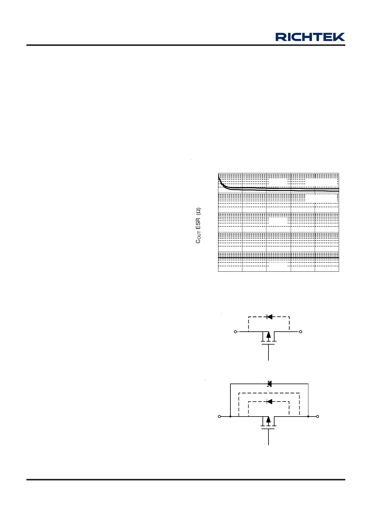
Note that some ceramic dielectrics exhibit large
capacitance and ESR variation with temperature. It may
be necessary to use 2.2μF or more to ensure stability at
temperatures below -10°C in this case. Also, tantalum
capacitors, 2.2μF or more may be needed to maintain
capacitance and ESR in the stable region for strict
application environment.
Tantalum capacitors maybe suffer failure due to surge
current when it is connected to a low-impedance source
of power (like a battery or very large capacitor). If a
tantalum capacitor is used at the input, it must be
guaranteed to have a surge current rating sufficient for
the application by the manufacture.
Load-Transient Considerations
The RT9182 load-transient response graphs show two
components of the output response: a DC shift from the
output impedance due to the load current change, and
the transient response. The DC shift is quite small due
to the excellent load regulation of the IC. Typical output
voltage transient spike for a step change in the load
current from 0mA to 50mA is tens mV, depending on the
ESR of the output capacitor. Increasing the output
capacitor's value and decreasing the ESR attenuates the
overshoot.
Input-Output (Dropout) Voltage
A regulator's minimum input-output voltage differential
(or dropout voltage) determines the lowest usable supply
voltage. In battery-powered systems, this will determine
the useful end-of-life battery voltage. Because the
RT9182 uses a P-Channel MOSFET pass transistor, the
dropout voltage is a function of drain-to-source on-
resistance [RDS(ON)] multiplied by the load current.
Reverse Current Path
The power transistor used in the RT9182 has an inherent
diode connected between each regulator input and output
(see Figure2). If the output is forced above the input by
more than a diode-drop, this diode will become forward
biased and current will flow from the VOUT terminal to
VIN. This diode will also be turned on by abruptly stepping
the input voltage to a value below the output voltage. To
prevent regulator mis-operation, a Schottky diode could
be used in the applications where input/output voltage
conditions can cause the internal diode to be turned on
(see Figure3). As shown, the Schottky diode is connected
in parallel with the internal parasitic diode and prevents
it from being turned on by limiting the voltage drop across
it to about 0.3V < 100mA to prevent damage to the part.
Region of Stable Cout ESR v.s Load Current
100
Instable
COUT = 4.7uF
10
COUT = 1uF
1
Stable
0.1
0.01
0.001
0
Instable
40
80
120
160
200
Load Current (mA)
Figure 1
VIN
VOUT
Figure 2
VIN
VOUT
Figure 3
www.richtek.com
8
DS9182-17 March 2007
Share Link: 