PI5C32X2383 Просмотр технического описания (PDF) - Pericom Semiconductor
Номер в каталоге
Компоненты Описание
Список матч
PI5C32X2383 Datasheet PDF : 4 Pages
| |||
PI5C32X383/PI5C32X2383
1122334455667788990011223344556677889900112233445566778899001122112233445566778899001122334455667788990011223344556677889900112211223344556677889900112233445566778899001122334455667788990011221122334455667788990011223344556677889900112233445566778899001122112233445566778899001122
Product Features
Near-zero propagation delay
Low noise, 25Ω version (PI5C32X2383)
5W switches connect inputs to outputs (PI5C32X383)
Direct bus connection when switches are ON
Ultra-low quiescent power (0.2µA typical)
Ideally suited for notebook applications
20-Bit Bus Switch/Exchange
Product Description
Pericom Semiconductors PI5C series of logic circuits are pro-
duced in the Companys advanced 0.8 micron CMOS technology,
achieving industry leading performance.
The PI5C32X383 and PI5C32X2383 are 20-bit bus switches with
exchange designed with a low ON resistance allowing inputs to be
connected directly to outputs. The bus switch creates no additional
Packages available:
propagational delay or additional ground bounce noise. The switches
48-pin 240-mil wide thin plastic TSSOP (A)
are turned ON by the Bus Enable (BE) input signal, and the Bus
48-pin 150-mil wide plastic QSOP (B)
Exchange (BX) input signal offers nibble swapping of the AB and
CD pairs of signals. This exchange configuration allows byte
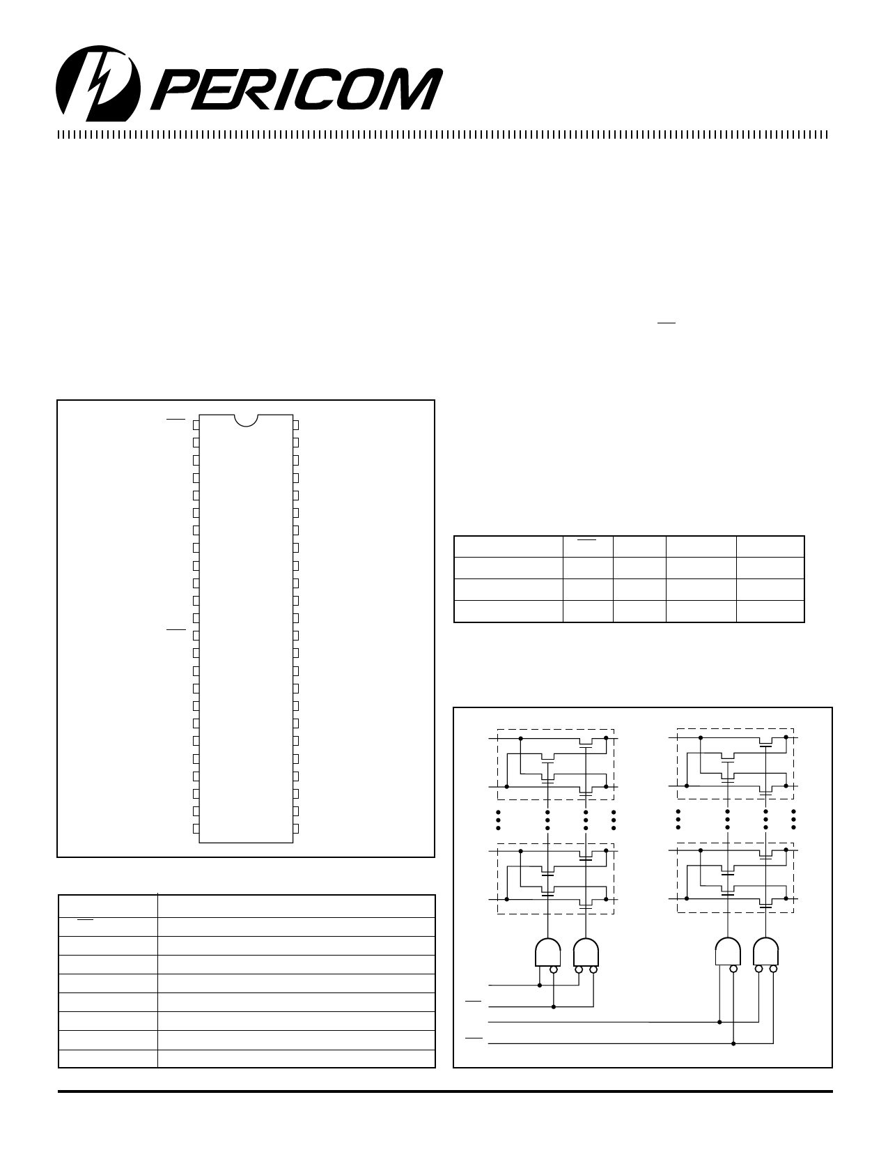
Product Pin Configuration
swapping of buses in systems. It can also be used as a quad
2-to-1 multiplexer and to create low delay barrel shifters, etc. The
BE1 1
C0 2
48 VCC
47 D4
PI5C32X2383 is designed with an internal 25Ω resistor reducing
noise reflection in high-speed applications.
A0 3
B0 4
D0 5
46 B4
45 A4
44 C4
Applications
10-wide 2:1 MUX, Byte Swapping, and Hot Insertion.
C1 6
A1 7
43 D3
42 B3
Truth Table(1)
B1 8
41 A3
Function
BEN BXn A0-A9 B0-B9
D1 9
40 C3
C2 10
39 D2
A2 11 48-Pin 38 B2
GND 12
37 BX1
Disconnect
Connect
Exchange
HX
Hi-Z
Hi-Z
L
L
C0-C9 D0-D9
L
H
D0-D9 C0-C9
BE2 13
C5 14
36 VCC
35 D9
Note: 1. H = High Voltage Level, X = Don’t Care,
L = Low Voltage Level, Hi-Z = High Impedance
A5 15
34 B9
B5 16
33 A9
Logic Block Diagram
D5 17
32 C9
C6 18
31 D8
A6 19
30 B8
A0
C0 A5
C5
B6 20
29 A8
D6 21
C7 22
28 C8
27 D7
B0
D0 B5
D5
A7 23
26 B7
GND 24
25 BX2
A4
C4 A9
C9
Product Pin Description
Pin Name
Description
B4
D4 B9
D9
BEn
Bus Enable Input (Active LOW)
BXn
Bus Exchange Input
Ax
Bus A
Bx
Bus B
BX1
Cx
Bus C
BE1
Dx
Bus D
BX2
GND
Ground
BE2
VCC
Power
1
PS8100 07/10/97
Share Link: 