CY7C1041CV33(2002) Просмотр технического описания (PDF) - Cypress Semiconductor
Номер в каталоге
Компоненты Описание
Список матч
CY7C1041CV33 Datasheet PDF : 11 Pages
| |||
CY7C1041CV33
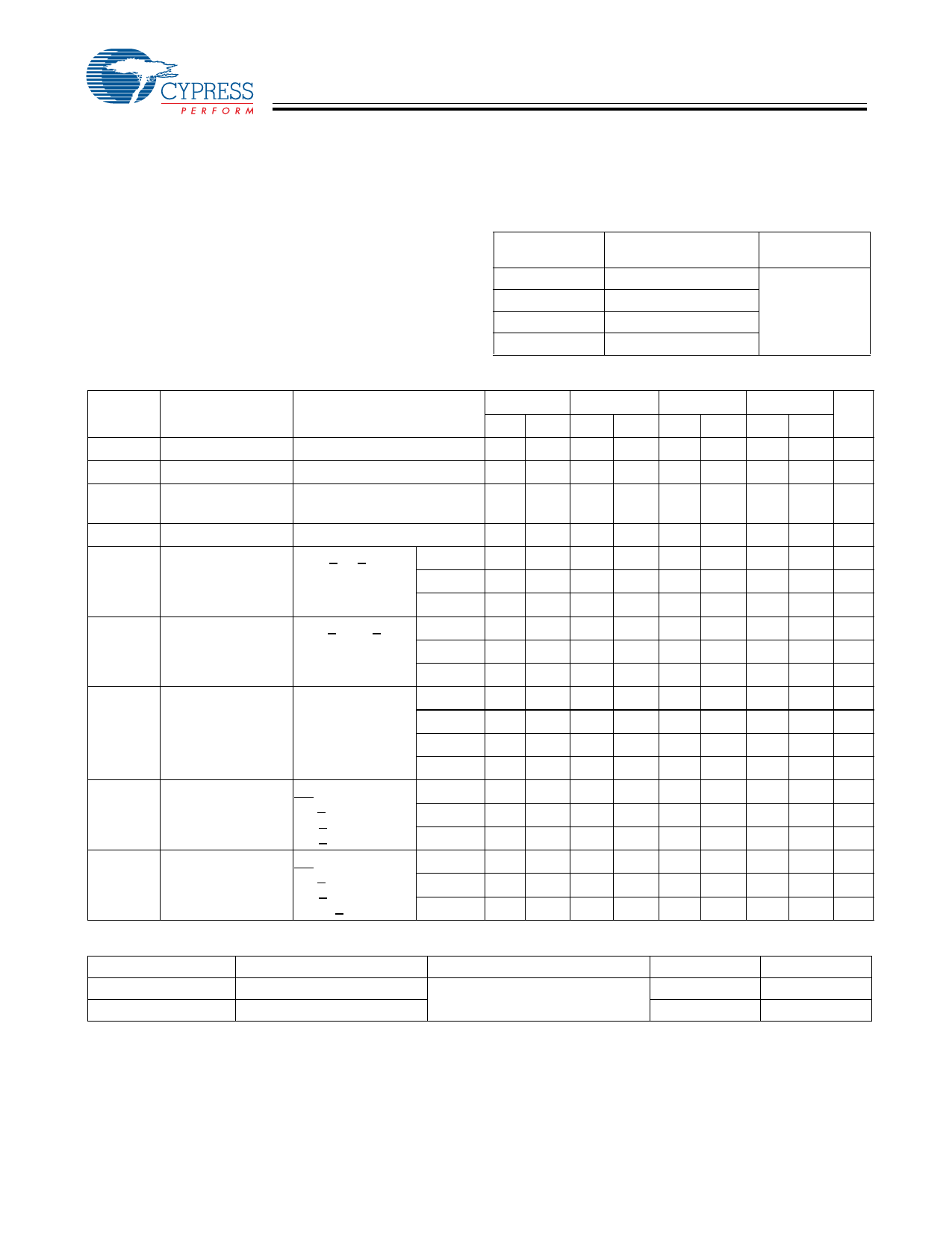
AC Switching Characteristics[4] Over the Operating Range
-8
-10
-12
-15
-20
Parameter
Description
Min. Max. Min. Max. Min. Max. Min. Max. Min. Max. Unit
Read Cycle
tpower[5]
VCC(typical) to the first access 1
tRC
Read Cycle Time
8
tAA
Address to Data Valid
tOHA
Data Hold from Address Change 3
tACE
CE LOW to Data Valid
tDOE
OE LOW to Data Valid
tLZOE
OE LOW to Low-Z
0
tHZOE
OE HIGH to High-Z[6, 7]
tLZCE
CE LOW to Low-Z[7]
3
tHZCE
CE HIGH to High-Z[6, 7]
tPU
CE LOW to Power-Up
0
tPD
CE HIGH to Power-Down
tDBE
Byte Enable to Data Valid
tLZBE
Byte Enable to Low-Z
0
tHZBE
Byte Disable to High-Z
Write Cycle[8, 9]
1
1
1
1
µs
10
12
15
20
ns
8
10
12
15
20 ns
3
3
3
3
ns
8
10
12
15
20 ns
4
5
6
7
8 ns
0
0
0
0
ns
4
5
6
7
8 ns
3
3
3
3
ns
4
5
6
7
8 ns
0
0
0
0
ns
8
10
12
15
20 ns
4
5
6
7
8 ns
0
0
0
0
ns
6
6
6
7
8 ns
tWC
Write Cycle Time
8
10
12
15
20
ns
tSCE
CE LOW to Write End
6
7
8
10
10
ns
tAW
Address Set-Up to Write End
6
7
8
10
10
ns
tHA
Address Hold from Write End
0
0
0
0
0
ns
tSA
Address Set-Up to Write Start
0
0
0
0
0
ns
tPWE
WE Pulse Width
6
7
8
10
10
ns
tSD
Data Set-Up to Write End
4
5
6
7
8
ns
tHD
tLZWE
tHZWE
Data Hold from Write End
WE HIGH to Low-Z[7]
WE LOW to High-Z[6, 7]
0
0
0
0
0
ns
3
3
3
3
3
ns
4
5
6
7
8 ns
tBW
Byte Enable to End of Write
6
7
8
10
10
ns
Shaded areas contain advance information.
Notes:
4. Test conditions assume signal transition time of 3 ns or less, timing reference levels of 1.5V, input pulse levels of 0 to 3.0V.
5. tPOWER gives the minimum amount of time that the power supply should be at typical VCC values until the first memory access can be performed.
6. tHZOE, tHZCE, and tHZWE are specified with a load capacitance of 5 pF as in part (d) of AC Test Loads. Transition is measured ±500 mV from steady-state voltage.
7. At any given temperature and voltage condition, tHZCE is less than tLZCE, tHZOE is less than tLZOE, and tHZWE is less than tLZWE for any given device.
8. The internal Write time of the memory is defined by the overlap of CE LOW, and WE LOW. CE and WE must be LOW to initiate a Write, and the transition of
either of these signals can terminate the Write. The input data set-up and hold timing should be referenced to the leading edge of the signal that terminates
the Write.
9. The minimum Write cycle time for Write Cycle No. 3 (WE controlled, OE LOW) is the sum of tHZWE and tSD.
Document #: 38-05134 Rev. *D
Page 4 of 11
Share Link: 