EL7516IY Просмотр технического описания (PDF) - Renesas Electronics
Номер в каталоге
Компоненты Описание
Список матч
EL7516IY Datasheet PDF : 12 Pages
| |||
EL7516
where:
IL = MOSFET current limit
IL-AVG = average inductor current
IL = inductor ripple current
IL = V-----I--N-L------------V--V--O--O----+-+----V-V---D--D---I-IO--O---D-D---E-E--------–----fV--S--I--N-----
(EQ. 8)
VDIODE = Schottky diode forward voltage, typically, 0.6V
fS = switching frequency, 600kHz or 1.2MHz
IL-AVG = I-1-O---–--U---D-T--
(EQ. 9)
D = MOSFET turn-on ratio:
D = 1 – V-----O----U----T-----V+----I-V-N---D----I--O-----D----E--
(EQ. 10)
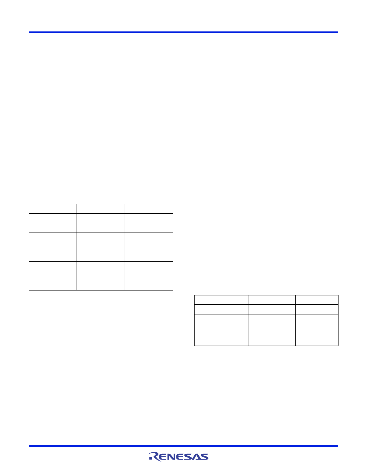
Table 1 gives typical maximum IOUT values for 1.2MHz
switching frequency and 22µH inductor:
VIN (V)
2.5
2.5
2.5
3.3
3.3
3.3
5
5
TABLE 1.
VOUT (V)
5
9
12
5
9
12
9
12
IOMAX (mA)
570
325
250
750
435
330
650
490
Thermal Performance
The EL7516 uses a fused-lead package, which has a
reduced JA of 100°C/W on a four-layer board and 115°C/W
on a two-layer board. Maximizing copper around the ground
pins will improve the thermal performance.
This device also has internal thermal shut-down set at
around +130°C to protect the component.
Layout Considerations
To achieve highest efficiency, best regulation and the most
stable operation, a good printed circuit board layout is
essential. It is strongly recommended that the demoboard
layout be followed as closely as possible. Use the following
general guidelines when laying out the print circuit board:
1. Place C4 as close to the VDD pin as possible. C4 is the
supply bypass capacitor of the device.
2. Keep the C1 ground, GND pin and C2 ground as close as
possible.
3. Keep the two high current paths a) from C1 through L1, to
the LX pin and GND and b) from C1 through L1, D1, and
C2 as short as possible.
4. High current traces should be as short and as wide as
possible.
5. Place the feedback resistor close to the FB pin to avoid
noise pickup.
6. Place the compensation network close to the COMP pin.
The demo board is a good example of layout based on these
principles; it is available upon request.
Differences Between EL7516 and ISL97516
ISL97516 is the replacement for EL7516, and it is pin-to-pin
compatible to EL7516, but there are differences between the
two parts, as shown in the Table 2:
TABLE 2. DIFFERENCES BETWEEN EL7516 AND ISL97516
ISL97516
EL7516
Current Limit
2.0A (typical value) 1.5A (typical value)
Over-Temperature
Protection
+150°C
+130°C
Logic High or Low Level Refer to Ground,
Fixed.
Refer to input
voltage, Varying
From Table 2, it shows that ISL97516 can provide more
output current at the same conditions, and work in higher
ambient temperature. The fixed logic level also helps reduce
the system design complexity.
FN7333 Rev 6.00
October 9, 2007
Page 11 of 12
Share Link: 