HTG12B0 Просмотр технического описания (PDF) - Holtek Semiconductor
Номер в каталоге
Компоненты Описание
Список матч
HTG12B0 Datasheet PDF : 33 Pages
| |||
HTG12B0
Absolute Maximum Ratings
Supply Voltage..............................-0.3V to 5.5V
Storage Temperature.................-50°C to 125°C
Input Voltage ......................VSS-0.3 to VDD+0.3
Operating Temperature ..................0°C to 70°C
Note: These are stress ratings only. Stresses exceeding the range specified under ²Absolute Maxi-
mum Ratings² may cause substantial damage to the device. Functional operation of this device
at other conditions beyond those listed in the specification is not implied and prolonged expo-
sure to extreme conditions may affect device reliability.
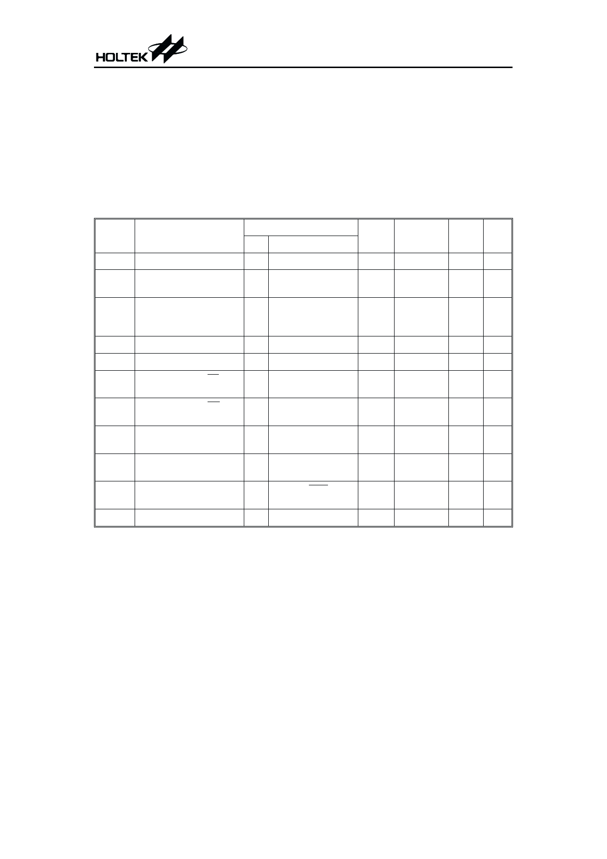
D.C. Characteristics
Symbol
Parameter
Test Conditions
VDD Conditions
VDD Operating Voltage
¾
¾
IDD
Operating Current
3V
No load,
fSYS=512kHz
ISTB
Standby Current,
(fSYS OFF and RTC ON, 3V Halt mode
LCD ON)
VIL
VIH
IOL1
Input Low Voltage
Input High Voltage
PA, PB, BZ and BZ
Output Sink Current
3V
¾
3V
¾
3V VOL=0.3V
IOH1
PA, PB, BZ and BZ
Output Source Current
3V VOH=2.7V
IOL2
IOH2
RPH
Segment Output Sink
Current
3V
VOL=0.44V
VLCD=4.4V
Segment Output Source
Current
3V
VOH=4.0V
VLCD=4.4V
Pull-high Resistor
3V
PS, PM, RES,
TMCLK
VLCD VLCD Output Voltage
3V
¾
Min.
2.4
¾
¾
0
0.8VDD
1.5
-0.5
100
30
50
3.96
Typ.
3
200
Ta=25°C
Max. Unit
3.6 V
300 mA
10
15 mA
¾
0.2VDD V
¾
VDD V
3
¾ mA
-1
¾ mA
200
¾ mA
60
¾ mA
100
150 kW
4.4
4.84 V
6
September 8, 1999
Share Link: 