ISL97642 Просмотр технического описания (PDF) - Renesas Electronics
Номер в каталоге
Компоненты Описание
Список матч
ISL97642 Datasheet PDF : 19 Pages
| |||
ISL97642
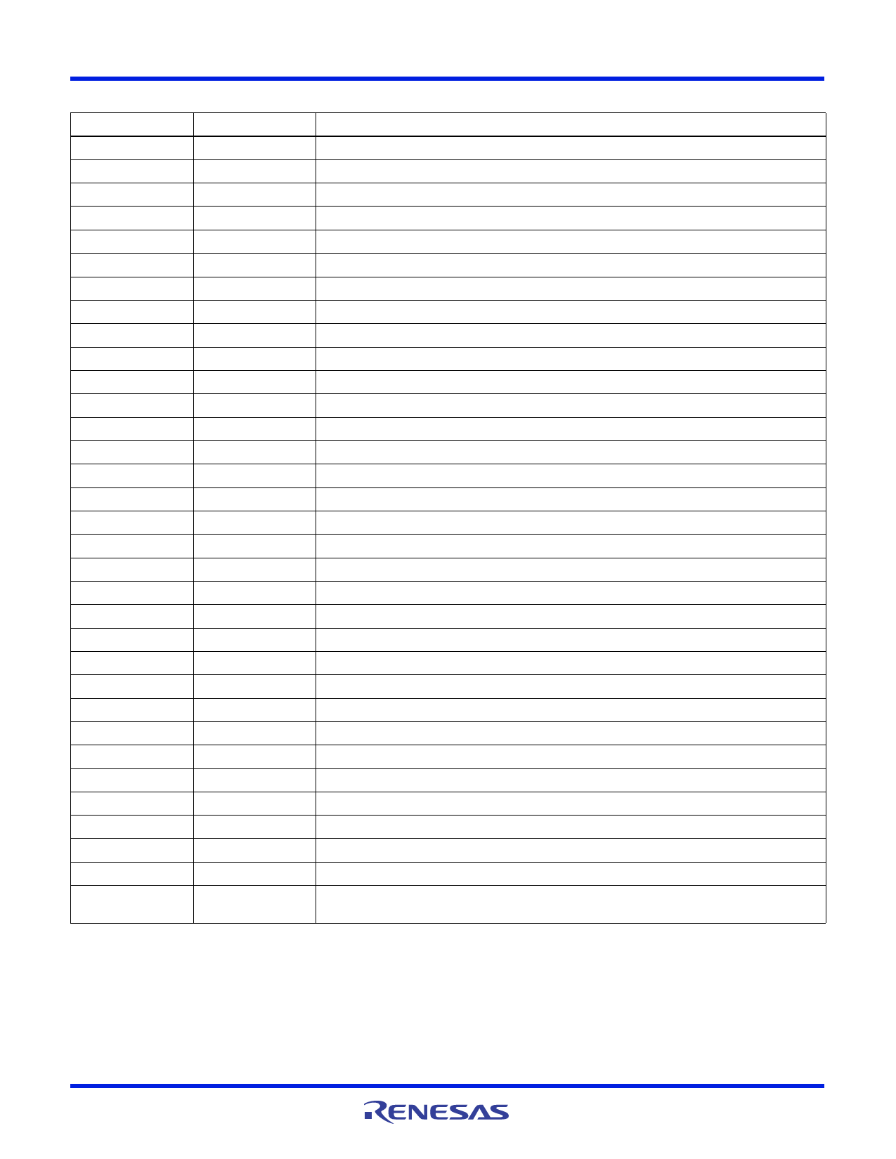
Pin Descriptions
PIN NAME
SRC
REF
AGND
PGND
OUT1
NEG1
POS1
OUT2
NEG2
POS2
BGND
POS3
NEG3
OUT3
SUP
POS3
NEG3
OUT3
NC
NC
NC
LX
IN
FB
COMP
FBP
DRVP
FBN
DRVN
DEL
CTL
DRN
COM
ISL97642
1
2
3
4
5
6
7
8
9
10
11
15
16
17
14
15
16
17
18
19
20
21
22
23
24
25
26
27
28
29
30
31
32
PIN FUNCTION
Upper reference voltage for switch output
Internal reference bypass terminal
Analog ground for boost converter and control circuitry
Power ground for boost switch
Operational amplifier 1 output
Operational amplifier 1 inverting input
Operational amplifier 1 non-inverting input
Operational amplifier 2 output
Operational amplifier 2 inverting input
Operational amplifier 2 non-inverting input
Operational amplifier ground
Operational amplifier 3 non-inverting input
Operational amplifier 3 inverting input
Operational amplifier 3 output
Amplifier positive supply rail. Bypass to BGND with 0.1µF capacitor
Operational amplifier 3 non-inverting input
Operational amplifier 3 inverting input
Operational amplifier 3 output
Main boost regulator switch connection
Main supply input; bypass to AGND with 1µF capacitor
Main boost feedback voltage connection
Error amplifier compensation pin
Positive LDO feedback connection
Positive LDO transistor drive
Negative LDO feedback connection
Negative LDO transistor driver
Connection for switch delay timing capacitor
Input control for switch output
Lower reference voltage for switch output
Switch output; when CTL = 1, COM is connected to SRC through a 15 resistor; when CTL = 0,
COM is connected to DRN through a 30 resistor
FN6436 Rev 0.00
June 18, 2007
Page 6 of 19
Share Link: 