L4936N Просмотр технического описания (PDF) - STMicroelectronics
Номер в каталоге
Компоненты Описание
Список матч
L4936N Datasheet PDF : 11 Pages
| |||
L4936N/NH
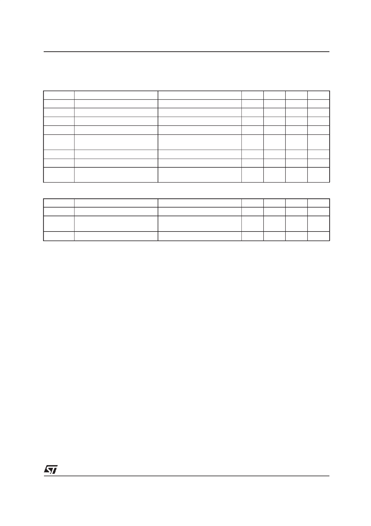
ELECTRICAL CHARACTERISTICS (continued)
RESET
Symbol
VRt
VRth
tRD
tRR
VRL
Parameter
Reset Low Threshold Voltage
Reset Threshold Hysteresis
Reset Pulse Delay
Reset Reaction Time
Reset Output LOW Voltage
ILRES
VCTh
VCTh, hyst
Reset Output HIGH Leakage
Delay Comparator Threshold
Delay Comparator Threshold
Hysteresis
SENSE
Test Conditions
VS = 14V
CT = 100nF; tR > 100µs
CT = 100nF
RRES = 10KΩ to V01
VS = 1.5V
VRES = 5V
Min.
Vo1 -0.4
50
55
1
Typ.
4.7
100
100
0
Max.
Vo1 -0.1
200
180
50
0.4
Unit
V
mV
mV
µs
V
1
µA
2.0
V
100
mV
VSlth
VSlth, hyst
VSOL
Sense Threshold Voltage
Sense Threshold Hysteresis
Sense Output LOW Voltage
ILSO Sense Output Leakage
VSI = 0.8V; VS ≥ 3V
RSO = 10KΩ to V01
VSO = 5V; VSI ≥ 1.5V
1.16 1.23 1.35
V
20
100 200 mV
0.4
V
1
µA
Note : 1 : VO2 connected to ADJ.VO2 can be set to higher values by inserting an external resistor divider.
2 : Foldback characteristic
FUNCTIONAL DESCRIPTION
The L4936N/NHare basedon the SGS-THOMSON
Microelectronics modular voltage regulator ap-
proach. Several out-standing features and auxiliary
functions are provided to meet the requirements of
supplyingthe microprocessorsystemsusedin auto-
motive applications.
Furthermore the device is suitable also in other ap-
plications requiring two stabilized voltages.
The modular approach allows other features and
functions to be realized easily when required.
STANDBY REGULATOR
The standby regulator uses an Isolated Collector
Vertical PNP transistor as the regulating element.
This structure allows a very low dropout voltage at
currents up to 50mA. The dropout operation of the
standby regulator is maintained down to 2V input
supply voltage. The output voltage is regulated up
tothe transient inputsupplyvoltage of 40V.This fea-
ture avoids functional interruptions which could be
generated by overvoltage pulses.
The typical curve of the standby output voltage as a
functionof the input supply voltage is shown in fig. 1.
The current consumption of the device (quiescent
current) is less than 250µA when output 2 is dis-
abled (standby mode). The dropout voltage is con-
trolled to reduce the quiescent current peak in the
undervoltage region and to improve the transient
response in this region.
The quiescent current is shownin fig. 2 as a function
of the supply input voltage 2.
OUTPUT 2 VOLTAGE
The output 2 regulator uses the same output struc-
ture as the standbyregulator, but rated for an output
current of 500mA.
The output 2 regulator works in tracking mode with
the standby output voltage as a reference voltage
when the output 2 programming pin ADJ is con-
nected to VO2. By connecting a resistor divider R1,
R2 to the pin ADJ as shown in fig. 3, the output volt-
age 2 can be programmed to the value :
VO2 = VO1 (1 + R1/R2)
The output 2 regulator can be switched off via the
Enable input.
5/11
Share Link: 