MC54HC597 Просмотр технического описания (PDF) - Motorola => Freescale
Номер в каталоге
Компоненты Описание
Список матч
MC54HC597
Motorola => Freescale

MC54HC597 Datasheet PDF : 9 Pages
| |||
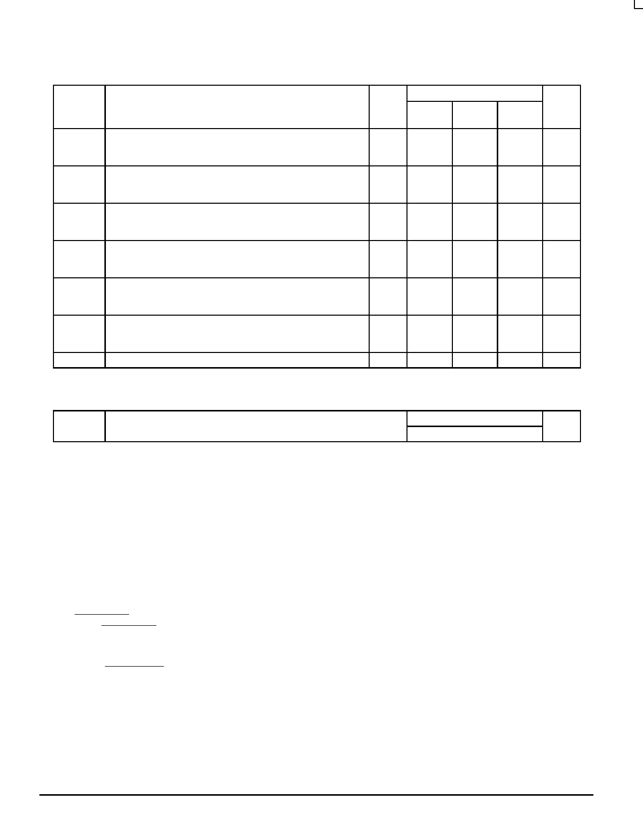
ÎÎÎÎÎÎÎÎÎÎÎÎÎÎÎÎÎÎÎÎÎÎÎÎÎÎÎÎÎÎÎÎÎÎÎÎÎÎÎÎÎÎÎÎÎÎÎÎÎÎÎÎÎÎÎÎÎÎÎÎÎÎÎÎÎÎ AC ELECTRICAL CHARACTERISTICS (CL = 50 pF, Input tr = tf = 6 ns)
ÎÎÎÎÎÎÎÎÎÎÎÎÎÎÎÎÎÎÎÎÎÎÎÎÎÎÎÎÎÎÎÎÎÎÎÎÎÎÎÎÎÎÎÎÎÎÎÎÎÎÎÎÎÎÎÎÎÎÎÎÎÎÎÎÎÎÎÎÎÎÎÎÎÎÎÎÎÎÎÎÎÎÎÎÎÎÎÎÎÎÎÎÎÎÎÎÎÎÎ Symbol
ÎÎÎÎÎÎÎÎÎÎÎÎÎÎÎÎÎÎÎÎÎÎÎÎÎÎÎÎÎÎÎÎÎ fmax
Parameter
Maximum Clock Frequency (50% Duty Cycle)
(Figures 2 and 8)
ÎÎÎÎÎÎÎÎÎÎÎÎÎÎÎÎÎÎÎÎÎÎÎÎÎÎÎÎÎÎÎÎÎÎÎÎÎÎÎÎÎÎÎÎÎÎÎÎÎÎÎÎÎÎÎÎÎÎÎÎÎÎÎÎÎÎ tPLH,
ÎÎÎÎÎÎÎÎÎÎÎÎÎÎÎÎÎÎÎÎÎÎÎÎÎÎÎÎÎÎÎÎÎ tPHL
Maximum Propagation Delay, Latch Clock to QH
(Figures 1 and 8)
ÎÎÎÎÎÎÎÎÎÎÎÎÎÎÎÎÎÎÎÎÎÎÎÎÎÎÎÎÎÎÎÎÎ tPLH,
ÎÎÎÎÎÎÎÎÎÎÎÎÎÎÎÎÎÎÎÎÎÎÎÎÎÎÎÎÎÎÎÎÎ tPHL
Maximum Propagation Delay, Shift Clock to QH
(Figures 2 and 8)
ÎÎÎÎÎÎÎÎÎÎÎÎÎÎÎÎÎÎÎÎÎÎÎÎÎÎÎÎÎÎÎÎÎÎÎÎÎÎÎÎÎÎÎÎÎÎÎÎÎÎÎÎÎÎÎÎÎÎÎÎÎÎÎÎÎÎ tPHL
Maximum Propagation Delay, Reset to QH
(Figures 3 and 8)
ÎÎÎÎÎÎÎÎÎÎÎÎÎÎÎÎÎÎÎÎÎÎÎÎÎÎÎÎÎÎÎÎÎÎÎÎÎÎÎÎÎÎÎÎÎÎÎÎÎÎÎÎÎÎÎÎÎÎÎÎÎÎÎÎÎÎ tPLH,
ÎÎÎÎÎÎÎÎÎÎÎÎÎÎÎÎÎÎÎÎÎÎÎÎÎÎÎÎÎÎÎÎÎ tPHL
Maximum Propagation Delay, Serial Shift/Parallel Load to QH
(Figures 4 and 8)
ÎÎÎÎÎÎÎÎÎÎÎÎÎÎÎÎÎÎÎÎÎÎÎÎÎÎÎÎÎÎÎÎÎ tTLH,
ÎÎÎÎÎÎÎÎÎÎÎÎÎÎÎÎÎÎÎÎÎÎÎÎÎÎÎÎÎÎÎÎÎ tTHL
Maximum Output Transition Time, Any Output
(Figures 1 and 8)
ÎÎÎÎÎÎÎÎÎÎÎÎÎÎÎÎÎÎÎÎÎÎÎÎÎÎÎÎÎÎÎÎÎÎÎÎÎÎÎÎÎÎÎÎÎÎÎÎÎÎÎÎÎÎÎÎÎÎÎÎÎÎÎÎÎÎ Cin
ÎÎÎÎÎÎÎÎÎÎÎÎÎÎÎÎÎÎÎÎÎÎÎÎÎÎÎÎÎÎÎÎÎ NOTES:
Maximum Input Capacitance
MC54/74HC597
VCC
V
2.0
4.5
6.0
2.0
4.5
6.0
2.0
4.5
6.0
2.0
4.5
6.0
2.0
4.5
6.0
2.0
4.5
6.0
—
Guaranteed Limit
v v – 55 to
25_C
85_C
125_C
6.0
4.8
4.0
30
24
20
35
28
24
210
265
315
42
53
63
36
45
54
175
220
265
35
44
53
30
37
45
175
220
265
35
44
53
30
37
45
175
220
265
35
44
53
30
37
45
75
95
110
15
19
22
13
16
19
10
10
10
Unit
MHz
ns
ns
ns
ns
ns
pF
1. For propagation delays with loads other than 50 pF, see Chapter 2 of the Motorola High–Speed CMOS Data Book (DL129/D).
2. Information on typical parametric values can be found in Chapter 2 of the Motorola High–Speed CMOS Data Book (DL129/D).
Typical @ 25°C, VCC = 5.0 V
CPD
Power Dissipation Capacitance (Per Package)*
50
pF
* Used to determine the no–load dynamic power consumption: PD = CPD VCC2f + ICC VCC. For load considerations, see Chapter 2 of the
Motorola High–Speed CMOS Data Book (DL129/D).
PIN DESCRIPTIONS
DATA INPUTS
A, B, C, D, E, F, G, H (Pins 15, 1, 2, 3, 4, 5, 6, 7)
Parallel data inputs. Data on these inputs is stored in the
input latch on the rising edge of the Latch Clock input.
SA (Pin 14)
Serial data input. Data on this input is shifted into the shift
register on the rising edge of the Shift Clock input it Serial
Shift/Parallel Load is high. Data on this input is ignored when
Serial Shift/Parallel Load is low.
CONTROL INPUTS
Serial Shift/Parallel Load (Pin 13)
Shift register mode control. When a high level is applied to
this pin, the shift register is allowed to serially shift data.
When a low level is applied to this pin, the shift register
accepts parallel data from the input latch, and serial shifting
is inhibited.
Reset (Pin 10)
Asynchronous, Active–low shift register reset. A low level
applied to this input resets the shift register to a low level, but
does not change the data in the input latch.
Shift Clock (Pin 11)
Serial shift register clock. A low–to–high transition on this
input shifts data on the Serial Data Input into the shift register
and data in stage H is shifted out QH, being replaced by the
data previously stored in stage G.
Latch Clock (Pin 12)
Latch clock. A low–to–high transition on this input loads
the parallel data on inputs A–H into the input latch.
OUTPUT
QH (Pin 9)
Serial data output. This pin is the output from the last stage
of the shift register.
High–Speed CMOS Logic Data
3
DL129 — Rev 6
MOTOROLA
Share Link: