R3111Q601B-TR-F Просмотр технического описания (PDF) - RICOH Co.,Ltd.
Номер в каталоге
Компоненты Описание
Список матч
R3111Q601B-TR-F Datasheet PDF : 44 Pages
| |||
R3111x
• Operation of R3111xxxxB
Ra
Rb
Vref
Rc
Comparator
VDD
OUT pin should be pulled-up to
OUT VDD or an external voltage level.
Nch
Tr.1
GND
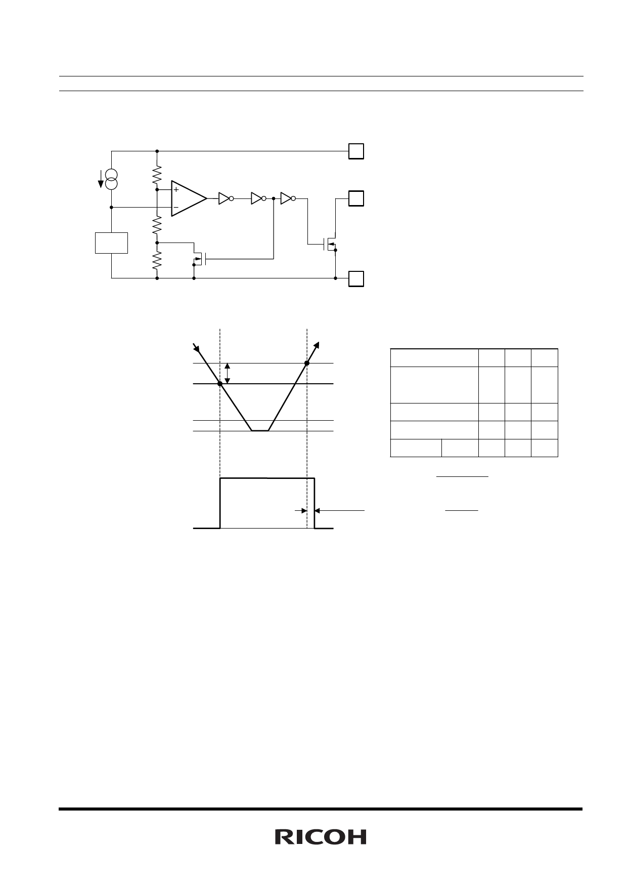
Block Diagram (R3111xxxxB)
1
2
3
Released Voltage +VDET
A
Detector Threshold -VDET
Supply Voltage
(VDD)
Minimum Operating Voltage VDDL
GND
Detector Threshold B
Hysteresis
Step
123
Comparator (+)
Pin Input Voltage
I II I
Comparator Output L H L
Tr.1
OFF ON OFF
Output Tr. Nch ON OFF ON
Pull-up Voltage
Output Voltage
(VOUT)
GND
Output
Delay Time
tPLH
Operation Diagram
I
Rb+Rc
Ra+Rb+Rc
×VDD
II
Rb
Ra+Rb
×VDD
• Explanation of operation
Step 1. The output voltage is equal to the GND level.
Step 2. At Point “A”, Vref >= VDD×(Rb+Rc)/(Ra+Rb+Rc) is true, as a result, the output of comparator is reversed
from "L" to "H", therefore the output voltage becomes the pull-up voltage. The voltage level of Point A
means a detector threshold voltage (−VDET).
Step 3. At Point “B”, Vref <= VDD×Rb/(Ra+Rb) is true, as a result, the output of comparator is reversed from "H" to
"L", then the output voltage is equal to the GND level. The voltage level of Point B means a released
voltage (+VDET).
∗) The difference between a released voltage and a detector threshold voltage is a detector threshold hysteresis.
15
Share Link: 