AIC1383 Просмотр технического описания (PDF) - Analog Intergrations
Номер в каталоге
Компоненты Описание
Список матч
AIC1383 Datasheet PDF : 7 Pages
| |||
AIC1383
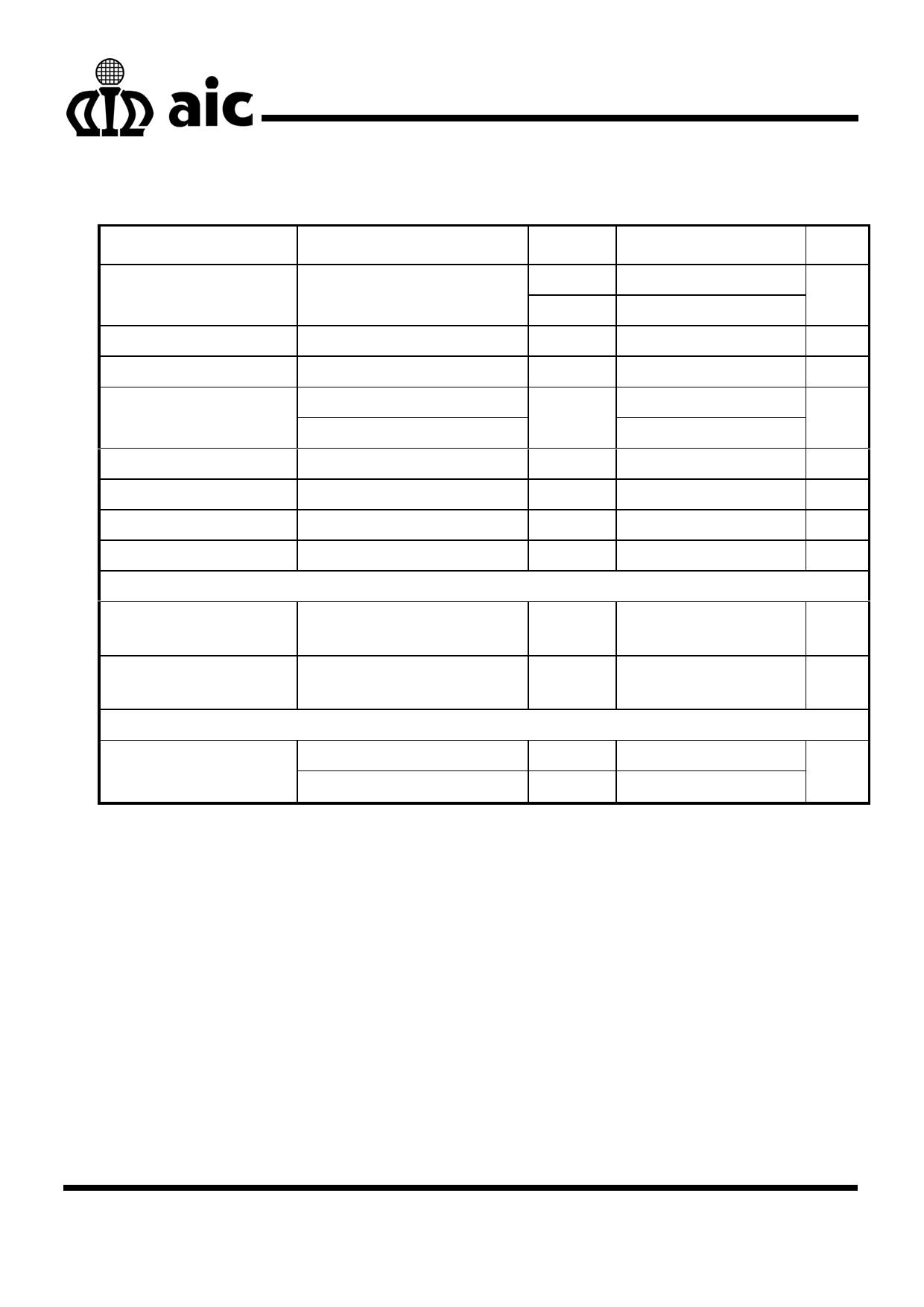
ELECTRICAL CHARACTERISTICS (VCNTL=3.3V, VIN=2.5V, VREF=0.5VIN,
COUT=10µF, TA=25°C, unless otherwise specified) (Note 1)
PARAMETER
TEST CONDITIONS
SYMBOL MIN. TYP. MAX.
UNIT
Input Voltage (DDR1/2)
Keep operate VCNTL≥VIN at
power on and off sequences
Output Voltage
IOUT = 0mA
Output Voltage Offset
IOUT = 0mA
IOUT =0.1mA ~ +1.5A
Load Regulation (DDR1/2)
IOUT = 0.1mA ~ -1.5A
Quiescent Current
VREF<0.2V, VOUT = OFF
Operating Current of VCNTL No load
VREF Bias Current
Current Limit
VREF=1.25V
THERMAL PROTECTION
VIN
1.6 2.5/1.8
V
VCNTL
3.0
3.3
6
VOUT
VREF
V
VOS
-20
20
mV
∆VLOR
10
25
mV
10
25
IQ
8
30
µA
ICNTL
3
10
mA
1
µA
IIL
2.1
3
4.5
A
Thermal Shutdown
Temperature
3.3V≤VCNTL≤5V
TSD
125 150
°C
Thermal Shutdown
Hysteresis
Guaranteed by design
30
°C
SHUTDOWN SPECIFICATIONS
Shutdown Threshold
Output ON (VREF=0V 1.25V)
Output OFF (VREF=1.25V 0V)
0.8
V
0.2
Note 1: Specifications are production tested at TA=25°C. Specifications over the -40°C to 85°C operating
temperature range are assured by design, characterization and correlation with Statistical Quality
Controls (SQC).
Note 2: VOS is the voltage measurement, which is defined as VOUT subtracted VREF.
Note 3: Load regulation is measured at constant junction temperature, using pulse testing with a low ON time.
Note 4: Current limit is measured by pulsing a short time.
Note 5: For operate system safely; VCNTL must be always greater than VIN.
3
Share Link: 