7CE12Z(2011) Просмотр технического описания (PDF) - NXP Semiconductors.
Номер в каталоге
Компоненты Описание
Список матч
7CE12Z Datasheet PDF : 21 Pages
| |||
NXP Semiconductors
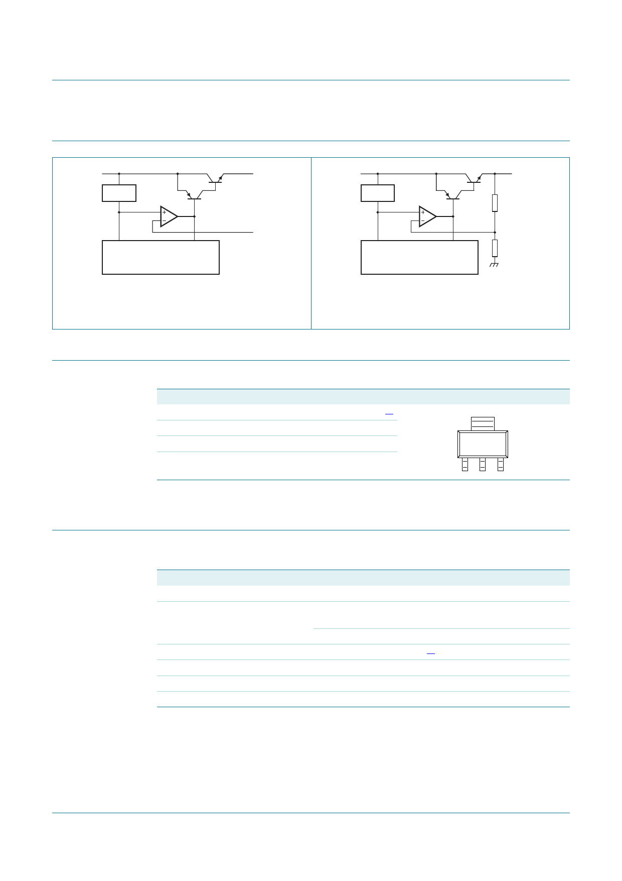
6. Functional diagram
NX1117C; NX1117CE series
Low-dropout linear regulators
VIN
Vref
VOUT
VIN
Vref
VOUT
ADJ
OUTPUT CURRENT LIMITING
SOA CONTROL
THERMAL SHUTDOWN
006aac638
Fig 1. Adjustable output voltage versions:
functional diagram
7. Pinning information
OUTPUT CURRENT LIMITING
SOA CONTROL
THERMAL SHUTDOWN
GND
006aac639
Fig 2. Fixed output voltage versions:
functional diagram
Table 4.
Pin
1
2
3
4
Pinning
Symbol
ADJ or GND
VOUT
VIN
VOUT
Description
adjust or ground
output
input
output
Simplified outline
[1]
4
123
[1] ADJ for NX1117CADJZ and NX1117CEADJZ; GND for all other devices.
8. Limiting values
Table 5. Limiting values
In accordance with the Absolute Maximum Rating System (IEC 60134).
Symbol Parameter
Conditions
Min
Max
Vin
input voltage
Ptot
total power dissipation
-
20
[1] internally limited
Tj
Tamb
Tstg
junction temperature
ambient temperature
storage temperature
-
150
40
+125
65
+150
[1]
The maximum package power dissipation is
Ptot
=
T----j---–----T----a---m---b- .
Rthj – a
Unit
V
C
C
C
NX1117C_NX1117CE_SER
Product data sheet
All information provided in this document is subject to legal disclaimers.
Rev. 1 — 18 July 2011
© NXP B.V. 2011. All rights reserved.
3 of 21
Share Link: 