MT8804A Просмотр технического описания (PDF) - Zarlink Semiconductor Inc
Номер в каталоге
Компоненты Описание
Список матч
MT8804A Datasheet PDF : 9 Pages
| |||
MT8804A CMOS
L2 1
L1 2
L0 3
D0 4
J0 5
D1 6
J1 7
D2 8
J2 9
D3 10
J3 11
VSS 12
24 VDD
23 L3
22 L4
21 L5
20 L6
19 L7
18 MR
17 AE
16 A2
15 A1
14 A0
13 VEE
24 PIN PLASTIC DIP
NC 5
•
25 L5
D0 6
24 L6
J0 7
23 L7
D1 8
22 MR
J1 9
21 AE
D2 10
20 A2
J2 11
19 NC
28 PIN PLCC
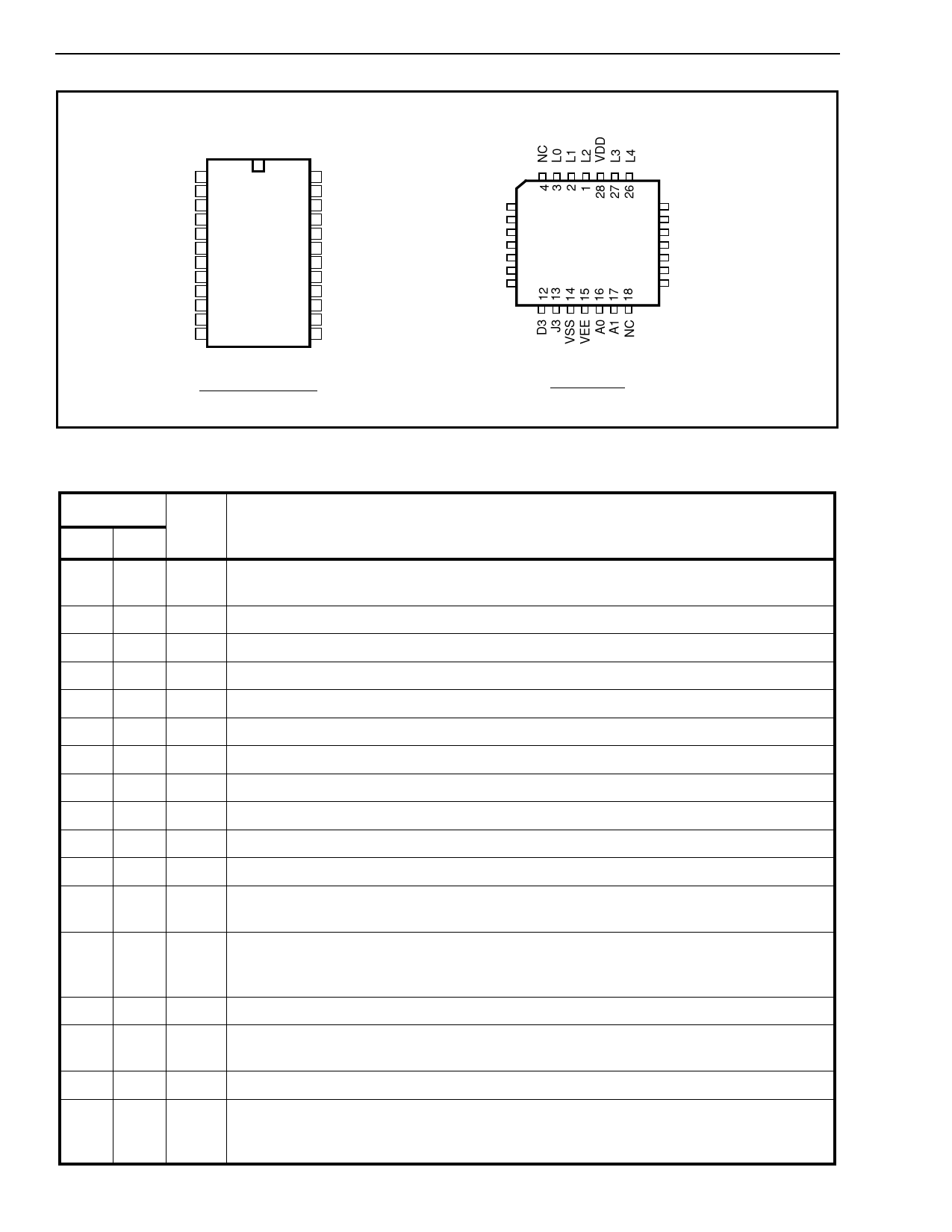
Pin Description
Figure 2 - Pin Connections
Pin #
Name
PDIP PLCC
Description
1-3 1-3 L2-L0 L2-L0 Analog Lines (Inputs/Outputs): These are connected to the L2-L0 columns of
the switch array.
4
6
D0 D0 Data (Input): Active High.
5
7
J0 J0 Analog Junctor (Input/Output). This is connected to the J0 row of the switch array.
6
8
DI DI Data (Input). Active High.
7
9
J1 J1 Analog Junctor (Input/Output). This is connected to the J1 row of the switch array.
8
10
D2 D2 Data (Input): Active High.
9
11
J2 J2 Analog Junctor (Input/Output). This is connected to the J2 row of the switch array.
10 12 D3 D3 Data (Input): Active High.
11 13 J3 J3 Analog Junctor (Input/Output). This is connected to the J3 row of the switch array.
12 14 VSS Digital Ground Reference.
13 15 VEE Negative Power Supply.
14-16 16,17, A0-A2 A0-A2 Address Lines (Inputs).
20
17 21 AE Address Enable/Strobe (Input). Enables function selected by address and data.
Address must be stable before AE goes high and D0-D3 must be stable on the falling
edge of the AE. Active High.
18 22 MR Master RESET (Input). This is used to turn off all switches. Active High.
19-23 23-27 L7-L3 L7-L3 Analog Lines (Inputs/Outputs). These are connected to the L7-L3 columns of
the switch array.
24 28 VDD Positive Power Supply.
4,
5,18,
19,
NC No Connect.
3-4
Share Link: 