3239-11 Просмотр технического описания (PDF) - Peregrine Semiconductor
Номер в каталоге
Компоненты Описание
Список матч
3239-11 Datasheet PDF : 12 Pages
| |||
PE3239
Product Specification
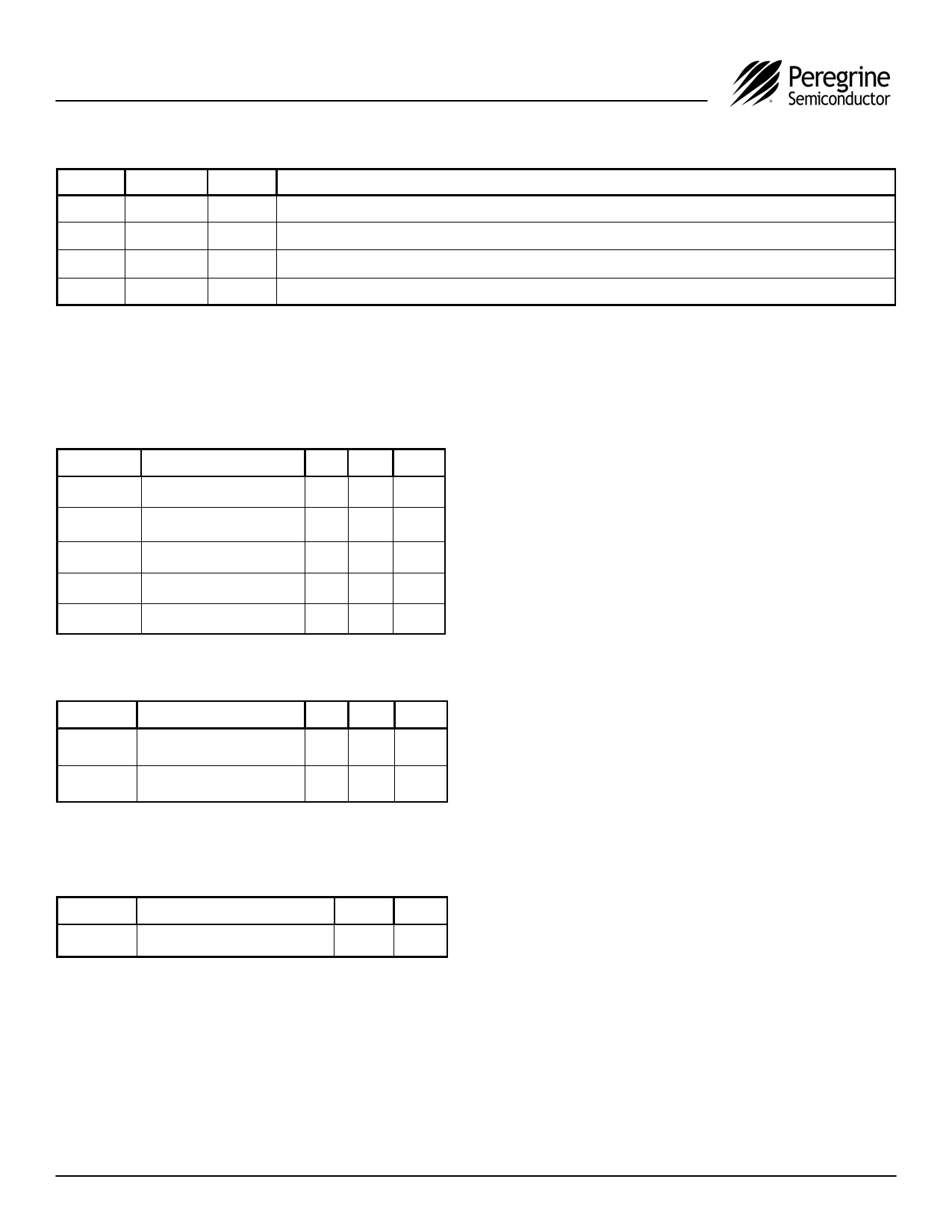
Table 1. Pin Descriptions (continued)
Pin No. Pin Name Type
Description
17
CP
18
NC
Output
Output
Charge pump current is sourced when fc leads fp and sinked when fc lags fp.
No connection.
19
GND
Ground.
20
fr
Input
Reference frequency input.
Note 1: VDD pins 1, 9, and 16 are connected by diodes and must be supplied with the same positive voltage level.
Table 2. Absolute Maximum Ratings
Symbol Parameter/Conditions Min Max Units
VDD
Supply voltage
VI
Voltage on any input
II
DC into any input
-0.3 4.0
V
-0.3
VDD +
0.3
V
-10 +10 mA
IO
DC into any output
-10 +10 mA
Tstg
Storage temperature range -65 150 °C
Table 3. Operating Ratings
Symbol Parameter/Conditions Min Max Units
VDD
Supply voltage
TA
Operating ambient
temperature range
2.85 3.15
V
-40 85
°C
Electrostatic Discharge (ESD) Precautions
When handling this UltraCMOS™ device, observe
the same precautions that you would use with
other ESD-sensitive devices. Although this device
contains circuitry to protect it from damage due to
ESD, precautions should be taken to avoid
exceeding the specified rating in Table 4.
Latch-Up Avoidance
Unlike conventional CMOS devices, UltraCMOS™
devices are immune to latch-up.
Table 4. ESD Ratings
Symbol
Parameter/Conditions
Level Units
VESD
ESD voltage human body model 1000
V
Note 1: Periodically sampled, not 100% tested. Tested per
MIL-STD-883, M3015 C2
Document No. 70-0047-02 │ www.psemi.com
©2006 Peregrine Semiconductor Corp. All rights reserved.
Page 3 of 12
Share Link: 