IDT71V256SA Просмотр технического описания (PDF) - Integrated Device Technology
Номер в каталоге
Компоненты Описание
Список матч
IDT71V256SA Datasheet PDF : 6 Pages
| |||
IDT71V256SA
3.3V CMOS STATIC RAM 256K (32K x 8-BIT)
INDUSTRIAL AND COMMERCIAL TEMPERATURE RANGES
AC ELECTRICAL CHARACTERISTICS (VCC = 3.3V ± 0.3V)
71V256SA10(2) 71V256SA12(2) 71V256SA15
Symbol
Parameter
Max. Min. Min. Max. Min. Max.
Read Cycle
tRC
Read Cycle Time
10
—
12
—
15
—
tAA
Address Access Time
—
10
—
12
—
15
tACS
tCLZ(1)
tCHZ(1)
Chip Select Access Time
Chip Select to Output in Low-Z
Chip Select to Output in High-Z
—
10
5
—
0
8
—
12
—
15
5
—
5
—
0
8
0
9
tOE
tOLZ(1)
tOHZ(1)
Output Enable to Output Valid
Output Enable to Output in Low-Z
Output Disable to Output in High-Z
—
6
3
—
2
6
—
6
—
7
3
—
0
—
2
6
0
7
tOH
Output Hold from Address Change
3
—
3
—
3
—
Write Cycle
tWC
Write Cycle Time
10
—
12
—
15
—
tAW
Address Valid to End-of-Write
9
—
9
—
10
—
tCW
Chip Select to End-of-Write
9
—
9
—
10
—
tAS
Address Set-up Time
0
—
0
—
0
—
tWP
Write Pulse Width
9
—
9
—
10
—
tWR
Write Recovery Time
0
—
0
—
0
—
tDW
Data to Write Time Overlap
6
—
6
—
7
—
tDH
tOW(1)
tWHZ(1)
Data Hold from Write Time
Output Active from End-of-Write
Write Enable to Output in High-Z
0
—
4
—
1
8
0
—
0
—
4
—
4
—
1
8
1
9
NOTE:
1. This parameter guaranteed with the AC test load (Figure 2) by device characterization, but is not production tested.
2. Commercial temperature range only.
71V256SA20(2)
Min. Max. Unit
20
—
ns
—
20
ns
—
20
ns
5
—
ns
0
10
ns
—
8
ns
0
—
ns
0
8
ns
3
—
ns
20
—
ns
15
—
ns
15
—
ns
0
—
ns
15
—
ns
0
—
ns
8
—
ns
0
—
ns
4
—
ns
1
10
ns
3101 tbl 10
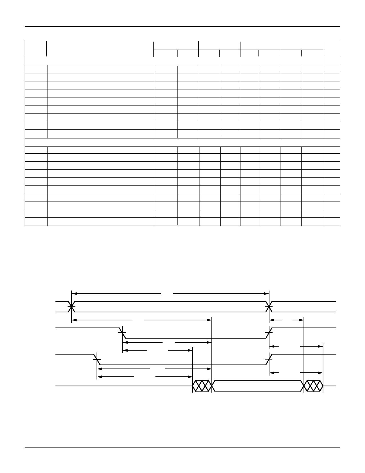
TIMING WAVEFORM OF READ CYCLE NO. 1(1)
t RC
ADDRESS
tAA
OE
CS
DATAOUT
tOE
t OLZ (2)
tACS
t CLZ (2)
NOTES:
1. WE is HIGH for Read cycle.
2. Transition is measured ±200mV from steady state.
tOH
t OHZ (2)
t CHZ (2)
DATA VALID
3101 drw 06
4
Share Link: 