IDT71256SA12PG Просмотр технического описания (PDF) - Integrated Device Technology
Номер в каталоге
Компоненты Описание
Список матч
IDT71256SA12PG Datasheet PDF : 8 Pages
| |||
IDT71256SA
CMOS Static RAM 256K (32K x 8-Bit)
Commercial and Industrial Temperature Ranges
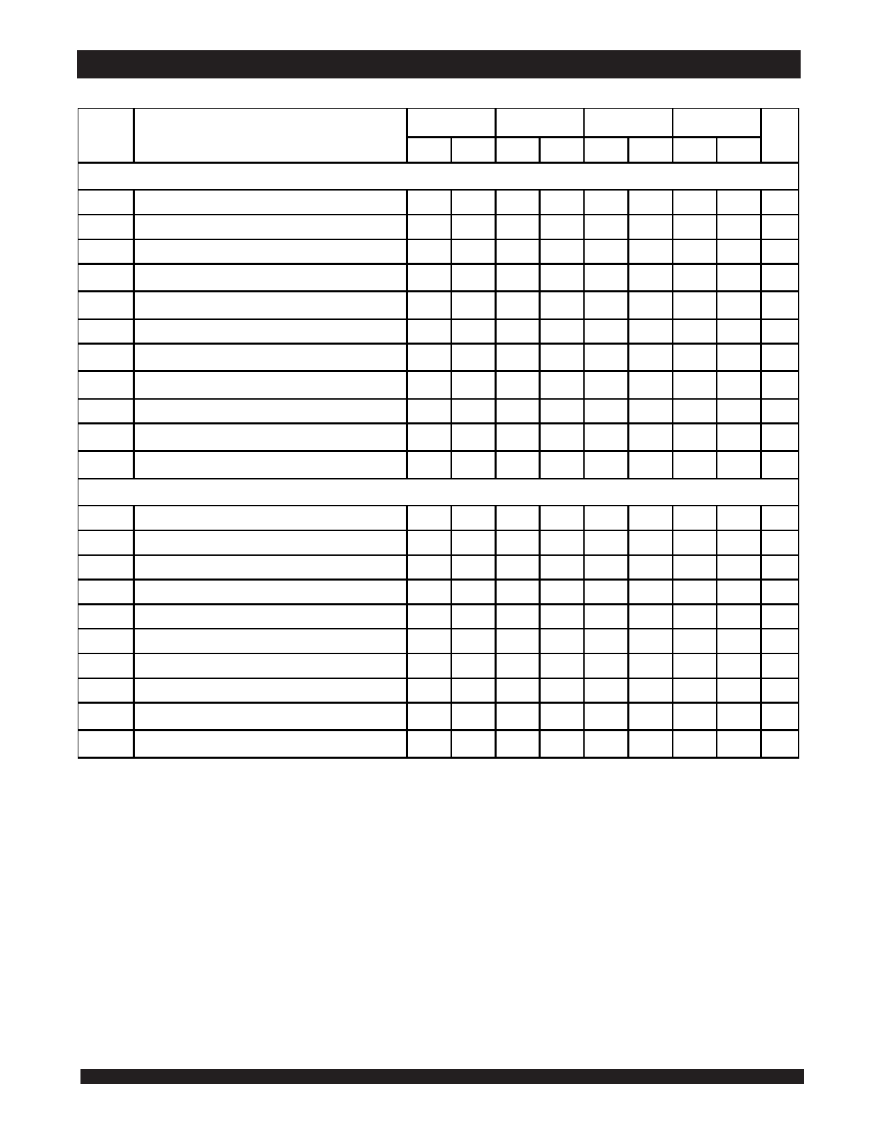
AC Electrical Characteristics (VCC = 5.0V ± 10%)
71256SA12
71256SA15
71256SA20
71256SA25
Symbol
Parameter
Min. Max. Min. Max. Min. Max. Min. Max. Unit
Read Cycle
tRC
Read Cycle Time
tAA
Address Access Time
tACS
Chip Select Access Time
tCLZ(1)
Chip Select to Output in Low-Z
12
____
15
____
20
____
25
____
ns
____
12
____
15
____
20
____
25 ns
____
12
____
15
____
20
____
25 ns
4
____
4
____
4
____
4
____
ns
tCHZ(1)
tOE
tOLZ(1)
Chip Sele ct to Output in High-Z
Output Enable to Output Valid
Output Enab le to Output in Low-Z
0
6
0
7
0
10
0
11 ns
____
6
____
7
____
10
____
11 ns
0
____
0
____
0
____
0
____
ns
tOHZ(1)
tOH
Output Disab le to Output in High-Z
Output Hold from Address Change
0
6
0
6
0
8
0
10 ns
3
____
3
____
3
____
3
____
ns
tPU(1)
Chip Sele ct to Power Up Time
0
____
0
____
0
____
0
____
ns
tPD(1)
Chip Deselect to Power Down Time
____
12
____
15
____
20
____
25 ns
Write Cycle
tWC
Write Cycle Time
tAW
Address Valid to End-of-Write
tCW
Chip Select to End-of-Write
tAS
Address Set-up Time
tWP
Write Pulse Width
tWR
Write Recovery Time
tDW
Data Valid to End-of-Write
tDH
Data Hold Time
tOW(1)
Output Active from End-of-Write
12
____
9
____
9
____
0
____
8
____
0
____
6
____
0
____
4
____
15
____
10
____
10
____
0
____
10
____
0
____
7
____
0
____
4
____
20
____
15
____
15
____
0
____
15
____
0
____
11
____
0
____
4
____
25
____
ns
20
____
ns
20
____
ns
0
____
ns
20
____
ns
0
____
ns
13
____
ns
0
____
ns
4
____
ns
tWHZ(1)
Write Enab le to Output in High-Z
0
6
0
6
0
NOTE:
1. This parameter is guaranteed with the AC Load (Figure 2) by device characterization, but is not production tested.
10
0
11 ns
2948 tbl 09
4
Share Link: 