HD74HC279 Просмотр технического описания (PDF) - Renesas Electronics
Номер в каталоге
Компоненты Описание
Список матч
HD74HC279 Datasheet PDF : 6 Pages
| |||
HD74HC279
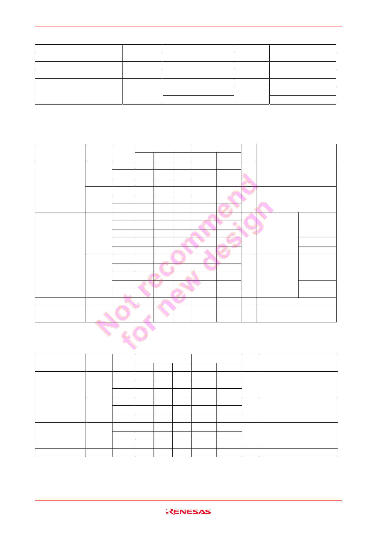
Recommended Operating Conditions
Item
Symbol
Ratings
Supply voltage
VCC
2 to 6
Input / Output voltage
VIN, VOUT
0 to VCC
Operating temperature
Input rise / fall time*1
Ta
–40 to 85
tr, tf
0 to 1000
0 to 500
0 to 400
Notes: 1. This item guarantees maximum limit when one input switches.
Waveform: Refer to test circuit of switching characteristics.
Unit
V
V
°C
ns
Conditions
VCC = 2.0 V
VCC = 4.5 V
VCC = 6.0 V
Electrical Characteristics
Item
Input voltage
Output voltage
Input current
Quiescent supply
current
Symbol
VIH
VIL
VOH
VOL
Iin
ICC
VCC (V)
2.0
4.5
6.0
2.0
4.5
6.0
2.0
4.5
6.0
4.5
6.0
2.0
4.5
6.0
4.5
6.0
6.0
6.0
Ta = 25°C
Min Typ Max
1.5 — —
3.15 — —
4.2 — —
— — 0.5
— — 1.35
— — 1.8
1.9 2.0 —
4.4 4.5 —
5.9 6.0 —
4.18 — —
5.68 — —
— 0.0 0.1
— 0.0 0.1
— 0.0 0.1
— — 0.26
— — 0.26
— — ±0.1
— — 2.0
Ta = –40 to+85°C
Unit
Min Max
Test Conditions
1.5
—
V
3.15
—
4.2
—
—
0.5 V
—
1.35
—
1.8
1.9
—
V Vin = VIH or VIL IOH = –20 µA
4.4
—
5.9
—
4.13
—
IOH = –4 mA
5.63
—
IOH = –5.2 mA
—
0.1
V Vin = VIH or VIL IOL = 20 µA
—
0.1
—
0.1
—
0.33
IOL = 4 mA
—
0.33
IOL = 5.2 mA
—
±1.0 µA Vin = VCC or GND
—
20 µA Vin = VCC or GND, Iout = 0 µA
Switching Characteristics
Item
Propagation delay
time
Output rise/fall
time
Input capacitance
Symbol VCC (V)
tPLH
2.0
tPHL
4.5
6.0
tPHL
2.0
4.5
6.0
tTLH
2.0
tTHL
4.5
6.0
Cin
—
Ta = 25°C
Min Typ Max
— — 130
— 10 26
— — 22
— — 120
— 12 24
— — 20
— — 75
— 5 15
— — 13
— 5 10
(CL = 50 pF, Input tr = tf = 6 ns)
Ta = –40 to +85°C
Unit
Min
Max
Test Conditions
—
165 ns S to Q
—
33
—
28
—
150 ns R to Q
—
30
—
26
—
95
ns
—
19
—
16
—
10 pF
Rev.2.00 Jan 31, 2006 page 3 of 5
Share Link: 