RC4153 Просмотр технического описания (PDF) - Fairchild Semiconductor
Номер в каталоге
Компоненты Описание
Список матч
RC4153 Datasheet PDF : 16 Pages
| |||
RC4153
Proper
Operation
PRODUCT SPECIFICATION
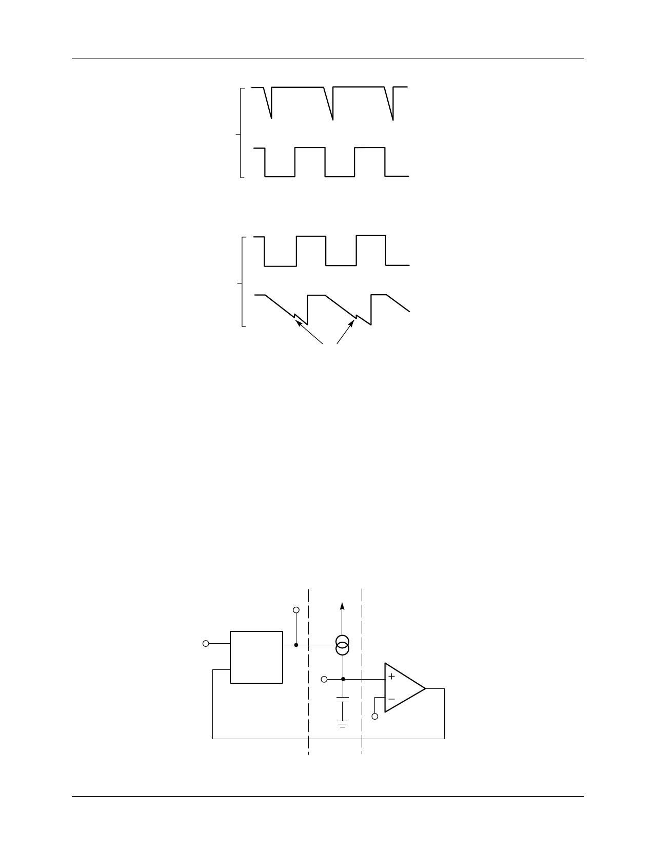
Timing
Waveform
on C O
Input
Frequency
Input
Frequency
Improper
Operation
Timing
Waveform
On C O
Gitch
4153-10
Figure 7. Frequency-to-Voltage Timing Waveforms
Detailed Circuit Operation
The circuit consists of a buried zener reference (breakdown
occurs below the surface of the die, reducing noise and
contamination), a high speed one-shot, a high speed
switched precision voltage-to-current converter and an
open-collector output transistor.
Figure 8 shows a block diagram of the high speed one-shot
and Figure 9 shows the monolithic implementation. A trigger
pulse sets the R-S latch, which lets CO charge from IT. When
the voltage on CO exceeds VTH. the comparator resets the
latch and discharges CO. Looking at the detailed schematic,
a positive trigger voltage turns on Q5, turns off Q4, and turns
on Q3. Q3 provides more drive to Q5 keeping it on and
latching the base of Q11 low. This turns on the switched
current source and turns off Q1, allowing CO to charge in a
negative direction. When the voltage on CO exceeds VTH,
Q13’s collector pulls Q3’s base down, resetting the latch,
turning off the switched current source and discharging CO
through Q1. Note that all of the transistors in the signal path
are NPNs, and that the voltage swings are minimized ECL
fashion to reduce delays. Minimum delay means minimum
drift of the resultant VFC scale factor at high frequency.
To Switched B
Current Source
C
Trig
Q
IT
Reset
D
CO
V TH
R-S Latch
Ramp
Gen
Comparator
Figure 8. One-Shot Block Diagram
4153-11
11
Share Link: 