UPD720122GC-9EU Просмотр технического описания (PDF) - NEC => Renesas Technology
Номер в каталоге
Компоненты Описание
Список матч
UPD720122GC-9EU Datasheet PDF : 82 Pages
| |||
µPD720122
2. ELECTRICAL SPECIFICATIONS
2.1 Buffer List
• 3.3 V oscillator interface
XIN,XOUT
• 3.3 V input buffer
FM21,SCAN(1:0)
• 5V torelant input buffer
RESETB,CSB,A(7:0),WRB,RDB,ACTIVE,EP1_DACKB,EP1_RDB,EP1_TCB,EP2_DACKB,EP2_WRB,
EP2_TCB,BUNRI,M0,M1,VBUS,ALE
• 5V torelant output buffer
INTB_ALL,INT0B,INT1B,INT2B,M2,EP1_DRQB,EP2_DRQB
• 5V torelant I/O buffer
D(15:0),LD(15:0),AD(7:0),D0,AD(7:1),D(15:8)
• USB interface
DP,DM,RSDP,RSDM,RREF,RPU
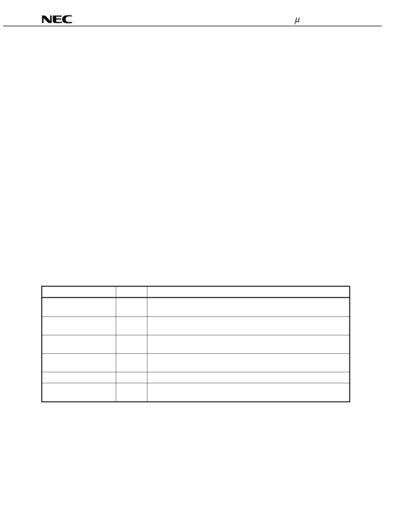
2.2 Terminology
Terms Used in Absolute Maximum Ratings
Parameter
Symbol
Meaning
Power supply voltage
VDD
Indicates voltage range within which damage or reduced reliability will not result
when power is applied to a VDD pin.
Input voltage
VI
Indicates voltage range within which damage or reduced reliability will not result
when power is applied to an input pin.
Output voltage
VO
Indicates voltage range within which damage or reduced reliability will not result
when power is applied to an output pin.
Output current
IO
Indicates absolute tolerance value for DC current to prevent damage or reduced
reliability when a current flows out of or into an output pin.
Operating temperature
TA
Storage temperature
Tstg
Indicates the ambient temperature range for normal logic operations.
Indicates the element temperature range within which damage or reduced reliability
will not result while no voltage or current are applied to the device.
Data Sheet S16685EJ2V0DS
11
Share Link: 