UPD448012-B55X Просмотр технического описания (PDF) - NEC => Renesas Technology
Номер в каталоге
Компоненты Описание
Список матч
UPD448012-B55X
NEC => Renesas Technology

UPD448012-B55X Datasheet PDF : 24 Pages
| |||
Electrical Specifications
µPD448012-X
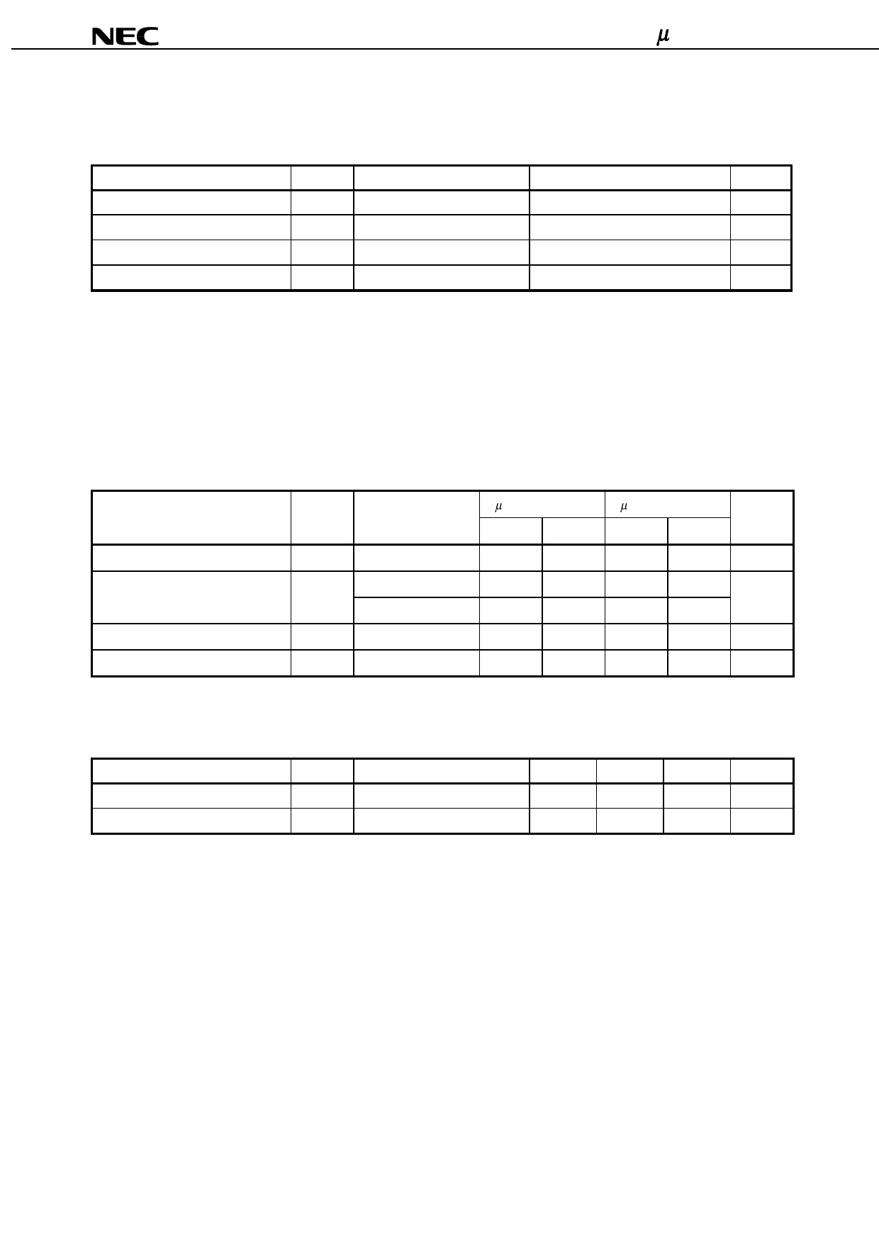
Absolute Maximum Ratings
Parameter
Supply voltage
Input / Output voltage
Operating ambient temperature
Storage temperature
Symbol
VCC
VT
TA
Tstg
Note –3.0 V (MIN.) (Pulse width : 30 ns)
Condition
Rating
Unit
–0.5 Note to +4.0
V
–0.5 Note to VCC + 0.4 (4.0 V MAX.)
V
–25 to +85
°C
–55 to +125
°C
Caution Exposing the device to stress above those listed in Absolute Maximum Rating could cause
permanent damage. The device is not meant to be operated under conditions outside the limits
described in the operational section of this specification. Exposure to Absolute Maximum Rating
conditions for extended periods may affect device reliability.
Recommended Operating Conditions
Parameter
Symbol
Condition
µPD448012-BxxX
µPD448012-CxxX
Unit
MIN.
MAX.
MIN.
MAX.
Supply voltage
High level input voltage
Low level input voltage
Operating ambient temperature
VCC
2.7
3.6
2.2
3.6
V
VIH
2.7 V ≤ VCC ≤ 3.6 V
2.4
VCC + 0.4
2.4
VCC + 0.4
V
2.2 V ≤ VCC < 2.7 V
–
–
2.0
VCC + 0.3
VIL
–0.3 Note
+0.5
–0.3 Note
+0.3
V
TA
–25
+85
–25
+85
°C
Note –1.5 V (MIN.) (Pulse width: 30 ns)
Capacitance (TA = 25°C, f = 1 MHz)
Parameter
Input capacitance
Input / Output capacitance
Symbol
CIN
CI/O
Test condition
VIN = 0 V
VI/O = 0 V
Remarks 1. VIN : Input voltage, VI/O : Input / Output voltage
2. These parameters are not 100% tested.
MIN.
TYP.
MAX.
Unit
8
pF
10
pF
Data Sheet M14466EJ5V0DS
5
Share Link: