RT9711AGF Просмотр технического описания (PDF) - Richtek Technology
Номер в каталоге
Компоненты Описание
Список матч
RT9711AGF Datasheet PDF : 17 Pages
| |||
RT9711A/B/C/D
Applications Information
The RT9711A/B/C/D are single N-MOSFET high-side
power switches with enable input, optimized for self-
powered and bus-powered Universal Serial Bus (USB)
applications. The RT9711 series are equipped with a
charge pump circuitry to drive the internal N-MOSFET
switch; the switch's low RDS(ON), 80mΩ, meets USB
voltage drop requirements; and a flag output is available
to indicate fault conditions to the local USB controller.
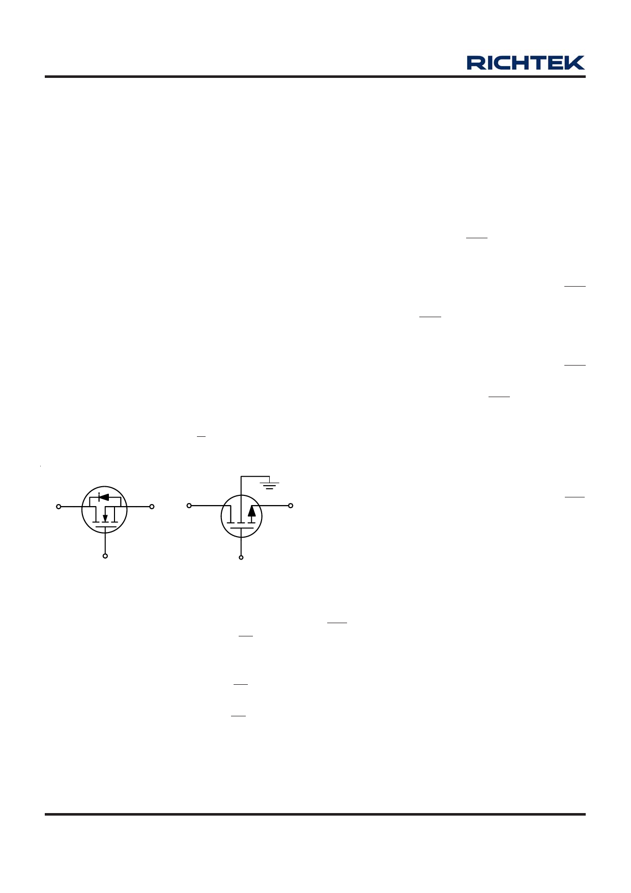
Input and Output
VIN (input) is the power source connection to the internal
circuitry and the drain of the MOSFET. VOUT (output) is
the source of the MOSFET. In a typical application, current
flows through the switch from VIN to VOUT toward the load.
If VOUT is greater than VIN, current will flow from VOUT to
VIN since the MOSFET is bidirectional when on.
Unlike a normal MOSFET, there is no a parasitic body
diode between drain and source of the MOSFET, the
RT9711A/B/C/D prevents reverse current flow if VOUT being
externally forced to a higher voltage than VIN when the
output disabled (VEN < 0.8V or VEN > 2V).
D
SD
S
G
Normal MOSFET
G
RT9711A/B/C/D
Chip Enable Input
The switch will be disabled when the EN/EN pin is in a
logic low/high condition. During this condition, the internal
circuitry and MOSFET are turned off, reducing the supply
current to 0.1μA typical. Floating the EN/EN may cause
unpredictable operation. EN should not be allowed to go
negative with respect to GND. The EN/EN pin may be
directly tied to VIN (GND) to keep the part on.
Soft Start for Hot Plug-In Applications
In order to eliminate the upstream voltage droop caused
by the large inrush current during hot-plug events, the
“soft-start” feature effectively isolates the power source
from extremely large capacitive loads, satisfying the USB
voltage droop requirements.
Fault Flag
The RT9711 series provides a FLG signal pin which is an
N-Channel open drain MOSFET output. This open drain
output goes low when VOUT < VIN − 1V, current limit or the
die temperature exceeds 130°C approximately. The FLG
output is capable of sinking a 10mA load to typically 200mV
above ground. The FLG pin requires a pull-up resistor,
this resistor should be large in value to reduce energy
drain. A 100kΩ pull-up resistor works well for most
applications. In the case of an over-current condition, FLG
will be asserted only after the flag response delay time,
tD, has elapsed. This ensures that FLG is asserted only
upon valid over-current conditions and that erroneous error
reporting is eliminated.
For example, false over-current conditions may occur
during hot-plug events when extremely large capacitive
loads are connected and causes a high transient inrush
current that exceeds the current limit threshold. The FLG
response delay time tD is typically 10ms.
Under-Voltage Lockout
Under-voltage lockout (UVLO) prevents the MOSFET
switch from turning on until input voltage exceeds
approximately 1.7V. If input voltage drops below
approximately 1.3V, UVLO turns off the MOSFET switch,
FLG will be asserted accordingly. Under-voltage detection
functions only when the switch is enabled.
Current Limiting and Short-Circuit Protection
The current limit circuitry prevents damage to the MOSFET
switch and the hub downstream port but can deliver load
current up to the current limit threshold of typically 2.5A
through the switch of RT9711A/B and 1A for RT9711C/D
respectively. When a heavy load or short circuit is applied
to an enabled switch, a large transient current may flow
until the current limit circuitry responds. Once this current
www.richtek.com
10
DS9711A/B/C/D-03 April 2011
Share Link: 