D8742 Просмотр технического описания (PDF) - Intel
Номер в каталоге
Компоненты Описание
Список матч
D8742 Datasheet PDF : 12 Pages
| |||
8742
Symbol
TEST 0
TEST 1
XTAL 1
XTAL 2
RESET
SS
CS
EA
RD
A0
WR
SYNC
D0 – D7
(BUS)
P10 – P17
P20 – P27
PROG
VCC
VDD
VSS
DIP
Pin
No
1
39
2
3
4
5
6
7
8
9
10
11
12 – 19
27 – 34
21 – 24
35– 38
25
40
26
20
Type
I
I
I
I
I
I
I
I
I
O
IO
IO
IO
IO
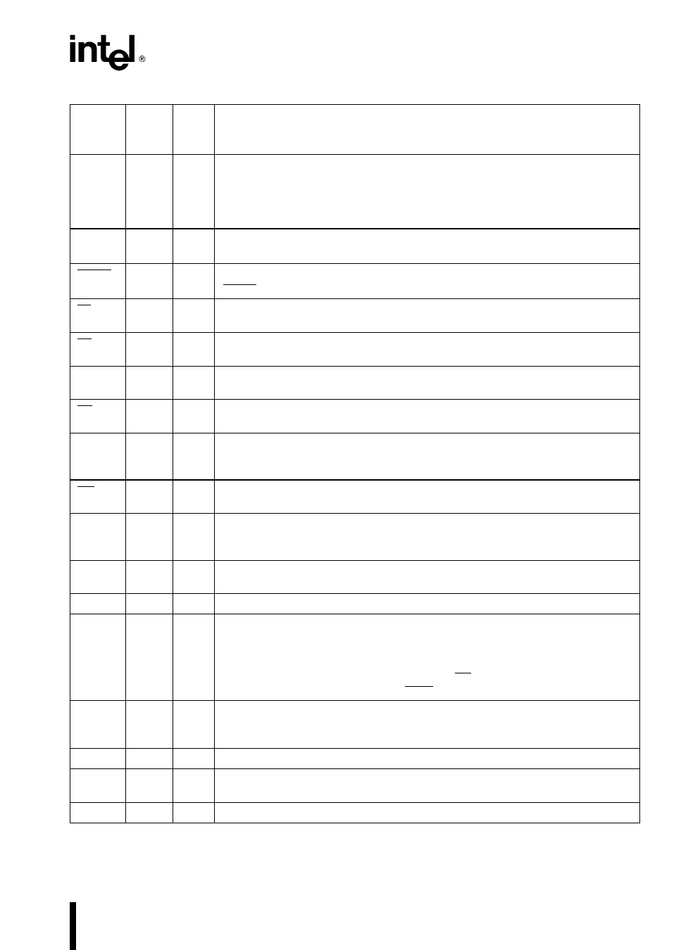
Table 1 Pin Description
Name and Function
TEST INPUTS Input pins which can be directly tested using conditional branch
instructions
FREQUENCY REFERENCE TEST 1 (T1) also functions as the event timer input (under
software control) TEST 0 (T0) is used during PROM programming and EPROM
verification
INPUTS Inputs for a crystal LC or an external timing signal to determine the internal
oscillator frequency
RESET Input used to reset status flip-flops and to set the program counter to zero
RESET is also used during EPROM programming and verification
SINGLE STEP Single step input used in conjunction with the SYNC output to step the
program through each instruction (EPROM) This should be tied to a5V when not used
CHIP SELECT Chip select input used to select one UPI microcomputer out of several
connected to a common data bus
EXTERNAL ACCESS External access input which allows emulation testing and EPROM
verification This pin should be tied low if unused
READ I O read input which enables the master CPU to read data and status words from
the OUTPUT DATA BUS BUFFER or status register
COMMAND DATA SELECT Address Input used by the master processor to indicate
whether byte transfer is data (A0 e 0 F1 is reset) or command (A0 e 1 F1 is set) A0 e 0
during program and verify operations
WRITE I O write input which enables the master CPU to write data and command words
to the UPI INPUT DATA BUS BUFFER
OUTPUT CLOCK Output signal which occurs once per UPI instruction cycle SYNC can
be used as a strobe for external circuitry it is also used to synchronize single step
operation
DATA BUS Three-state bidirectional DATA BUS BUFFER lines used to interface the UPI
microcomputer to an 8-bit master system data bus
PORT 1 8-bit PORT 1 quasi-bidirectional I O lines
PORT 2 8-bit PORT 2 quasi-bidirectional I O lines The lower 4 bits (P20 – P23) interface
directly to the 8243 I O expander device and contain address and data information during
PORT 4 – 7 access The upper 4 bits (P24 – P27) can be programmed to provide interrupt
Request and DMA Handshake capability Software control can configure P24 as Output
Buffer Full (OBF) interrupt P25 as Input Buffer Full (IBF) interrupt P26 as DMA Request
(DRQ) and P27 as DMA ACKnowledge (DACK)
PROGRAM Multifunction pin used as the program pulse input during PROM programming
During I O expander access the PROG pin acts as an address data strobe to the 8243
This pin should be tied high if unused
POWER a5V main power supply pin
POWER a5V during normal operation a21V during programming operation Low power
standby supply pin
GROUND Circuit ground potential
3
3
Share Link: 