DAP011 Просмотр технического описания (PDF) - ON Semiconductor
Номер в каталоге
Компоненты Описание
Список матч
DAP011 Datasheet PDF : 24 Pages
| |||
DAP011/DAP011C
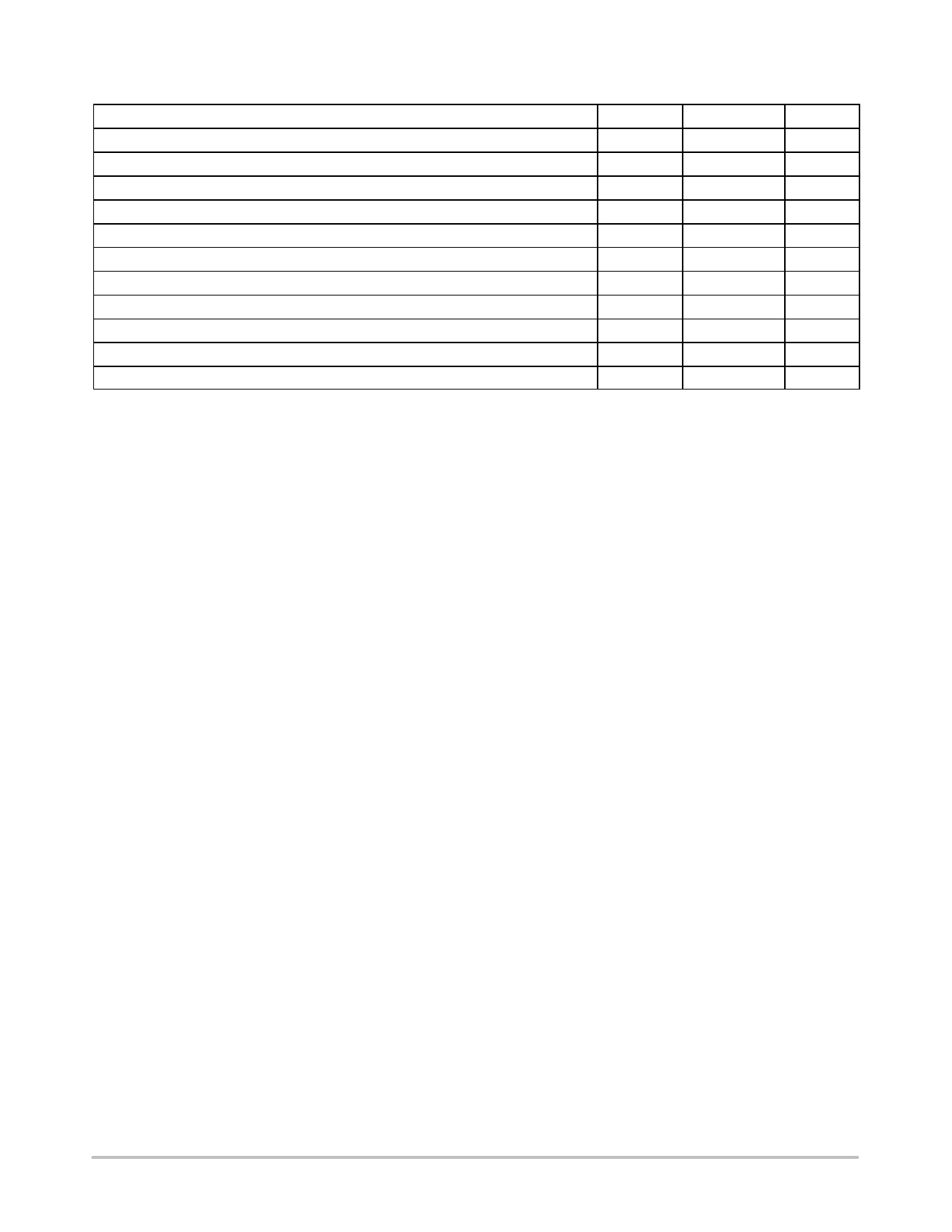
MAXIMUM RATINGS
Rating
Symbol
Value
Unit
Power Supply Voltage, VCC Pin, Continuous Voltage
Transient Power Supply Voltage, Duration < 10 ms, IVCC < 20 mA
Maximum Voltage on Low Power Pins (Except Pin 9, Pin 10, Pin 5 and Pin 14)
VCC
20
V
−
25
V
−
−0.3 to 10
V
Maximum Voltage on Pin 5
−
5.0
V
Thermal Resistance, Junction−to−Air
Thermal Reference Junction−to−Lead (Note 3)
Maximum Junction Temperature
Storage Temperature Range
RqJA
Psi JL
TJMAX
−
120
40
150
−60 to +150
°C/W
°C/W
°C
°C
ESD Capability, HBM Model (All Pins Except HV)
−
2.0
kV
ESD Capability, Machine Model
−
200
V
Maximum Voltage on Pin 14 (HV)
−
−0.3 to 500
V
Maximum ratings are those values beyond which device damage can occur. Maximum ratings applied to the device are individual stress limit
values (not normal operating conditions) and are not valid simultaneously. If these limits are exceeded, device functional operation is not implied,
damage may occur and reliability may be affected.
1. This device series contains ESD protection and exceeds the following tests: Human Body Model 2000 V per Mil−Std−883, Method 3015.
Machine Model Method 200 V
2. This device contains latch−up protection and exceeds 100 mA per JEDEC Standard JESD78.
3. Minimum Pad FR4 Board 1 oz Copper.
http://onsemi.com
4
Share Link: 