IDT2305(2007) Просмотр технического описания (PDF) - Integrated Device Technology
Номер в каталоге
Компоненты Описание
Список матч
IDT2305 Datasheet PDF : 11 Pages
| |||
IDT2305
3.3V ZERO DELAY CLOCK BUFFER
COMMERCIAL AND INDUSTRIAL TEMPERATURE RANGES
ZERO DELAY AND SKEW CONTROL
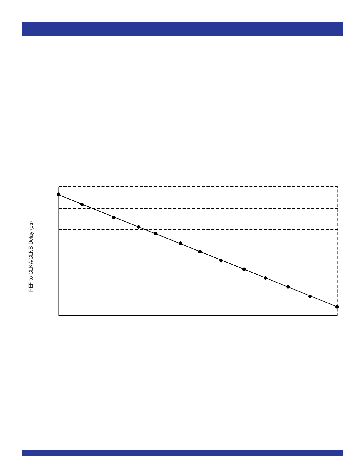
All outputs should be uniformly loaded in order to achieve Zero I/O Delay. Since the CLKOUT pin is the internal feedback for the PLL, its relative
loading can affect and adjust the input/output delay. The Output Load Difference diagram illustrates the PLL's relative loading with respect to the other
outputs that can adjust the Input-Output (I/O) Delay.
For designs utilizing zero I/O Delay, all outputs including CLKOUT must be equally loaded. Even if the output is not used, it must have a capacitive
load equal to that on the other outputs in order to obtain true zero I/O Delay. If I/O Delay adjustments are needed, use the Output Load Difference diagram
to calculate loading differences between the CLKOUT pin and other outputs. For zero output-to-output skew, all outputs must be loaded equally.
REF TO CLKA/CLKB RELAY vs. OUTPUT LOAD DIFFERENCE BETWEEN CLKOUT PIN AND CLKA/CLKB PINS
1500
1000
500
0
-30
-25
-20
-15
-10
-5
0
5
10
15
20
25
30
-500
-1000
-1500
OUTPUT LOAD DIFFERENCE BETWEEN CLKOUT PIN AND CLKA/CLKB PINS (pF)
6
Share Link: 