MSM6947GS-K Просмотр технического описания (PDF) - Oki Electric Industry
Номер в каталоге
Компоненты Описание
Список матч
MSM6947GS-K Datasheet PDF : 31 Pages
| |||
¡ Semiconductor
MSM6927/6947
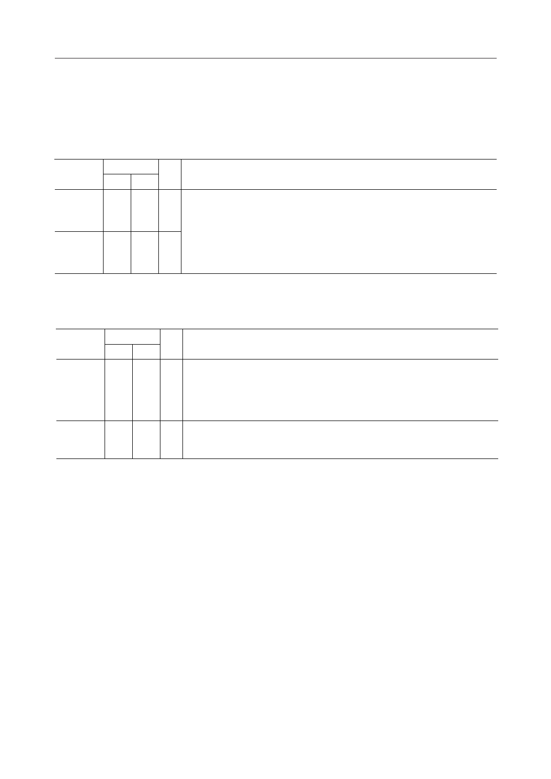
Both MSM6927RS (or GS-K) and MSM6947RS (or GS-K) have 28 (or 44) pins. The pin descriptions
for these 28 (or 44) pins are same except those for No. 27 (or No. 36) pin and No. 28 (or No. 38).
The pin descriptions for No. 27 (or No. 36) pin and No. 28 (or No. 38) pin are described as follows.
MSM6927
Name
TS1
TS2
Pin No.
I/O
RS GS-K
27 36 I
28 38 I
Description
RS/CS delay and carrier detect delay options referred to chapter about timing
characteristics are selected by TS1 and TS2 inputs. Be careful that each delay
can not be individually selected. If another delay time than the ones within the
device are required as an option, input a digital "High" to the TS1 and TS2 pin
and implement the external delay circuits to obtain the desired delay
characteristics. In this case, the CD2 pin becomes not only the input for the
external circuit output signal, but also the Carrier detect output. See Fig. 11-1.
MSM6947
Name
TS
ATE
Pin No.
I/O
RS GS-K
27 36 I
28 38 I
Description
When a digital "Low" is input to the TS pin, the built-in RS/CS, carrier detect and
receiver-squelch delay are provided. If another delay time is required, it can be
implemented by inputting a digital "High" to this pin and incorporates the external
delay circuits. In this case, the CD2 pin becomes not only the input for the
external circuit output signal, but also the Carrier detect output. See Fig. 11-2.
Answer tone enable input. When a digital "Low" is input to this pin and the RS1
pin is in the digital "Low" level, the Answer Tone (to 2025 Hz) is sent over the
phone line via the AO pin.
7/31
Share Link: 