2SK3498 Просмотр технического описания (PDF) - Toshiba
Номер в каталоге
Компоненты Описание
Список матч
2SK3498 Datasheet PDF : 3 Pages
| |||
2SK3498
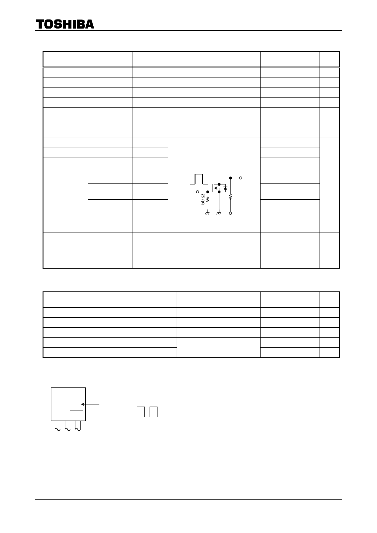
Electrical Characteristics (Tc = 25°C)
Characteristics
Gate leakage current
Drain-source breakdown voltage
Drain cut-OFF current
Drain-source breakdown voltage
Gate threshold voltage
Drain-source ON resistance
Forward transfer admittance
Input capacitance
Reverse transfer capacitance
Output capacitance
Rise time
Switching time
Turn-ON time
Fall time
Turn-OFF time
Total gate charge
(gate-source plus gate-drain)
Gate-source charge
Gate-drain (“miller”) charge
Symbol
Test Condition
Min Typ. Max Unit
IGSS
V (BR) GSS
VGS = ±25 V, VDS = 0 V
IG = ±10 µA, VDS = 0 V
±10
µA
±30
V
IDSS
V (BR) DSS
Vth
VDS = 400 V, VGS = 0 V
ID = 10 mA, VGS = 0 V
VDS = 10 V, ID = 1 mA
100
µA
450
V
2.0
4.0
V
RDS (ON) VGS = 10 V, ID = 0.5 A
4.2
5.5
Ω
Yfs
Ciss
Crss
VDS = 10 V, ID = 0.5 A
VDS = 10 V, VGS = 0 V, f = 1 MHz
0.3
0.6
S
145
35
pF
Coss
80
tr
VG1S0 V
0V
ton
tf
ID = 0.5 A VOUT
14
56
RL = 400 Ω
ns
26
toff
Duty <= 1%, tw = 10 µs VDD ∼− 200 V
75
Qg
Qgs
VDD ∼− 320 V, VGS = 10 V, ID = 1 A
Qgd
5.7
3.0
nC
2.7
Source-Drain Ratings and Characteristics (Tc = 25°C)
Characteristics
Continuous drain reverse current (Note 1)
Pulse drain reverse current
(Note 1)
Forward voltage (diode)
Reverse recovery time
Reverse recovery charge
Symbol
IDR
IDRP
VDSF
trr
Qrr
Test Condition
IDR = 1 A, VGS = 0 V
IDR = 1 A, VGS = 0 V,
dIDR/dt = 100 A/µs
Min Typ. Max Unit
1
A
3
A
−1.7
V
650
ns
14.6
µC
Marking
K3498
※
Type
※ Lot Number
Month (starting from alphabet A)
Year (last number of the christian era)
2
2002-02-27
Share Link: 