ADV7612 Просмотр технического описания (PDF) - Analog Devices
Номер в каталоге
Компоненты Описание
Список матч
ADV7612 Datasheet PDF : 20 Pages
| |||
ADV7612
Data Sheet
SPECIFICATIONS
At DVDD = 1.71 V to 1.89 V, DVDDIO = 3.14 V to 3.46 V, PVDD = 1.71 V to 1.89 V, TVDD = 3.14 V to 3.46 V, CVDD = 1.71 V to 1.89 V,
Operating temperature range, unless otherwise noted.
ELECTRICAL CHARACTERISTICS
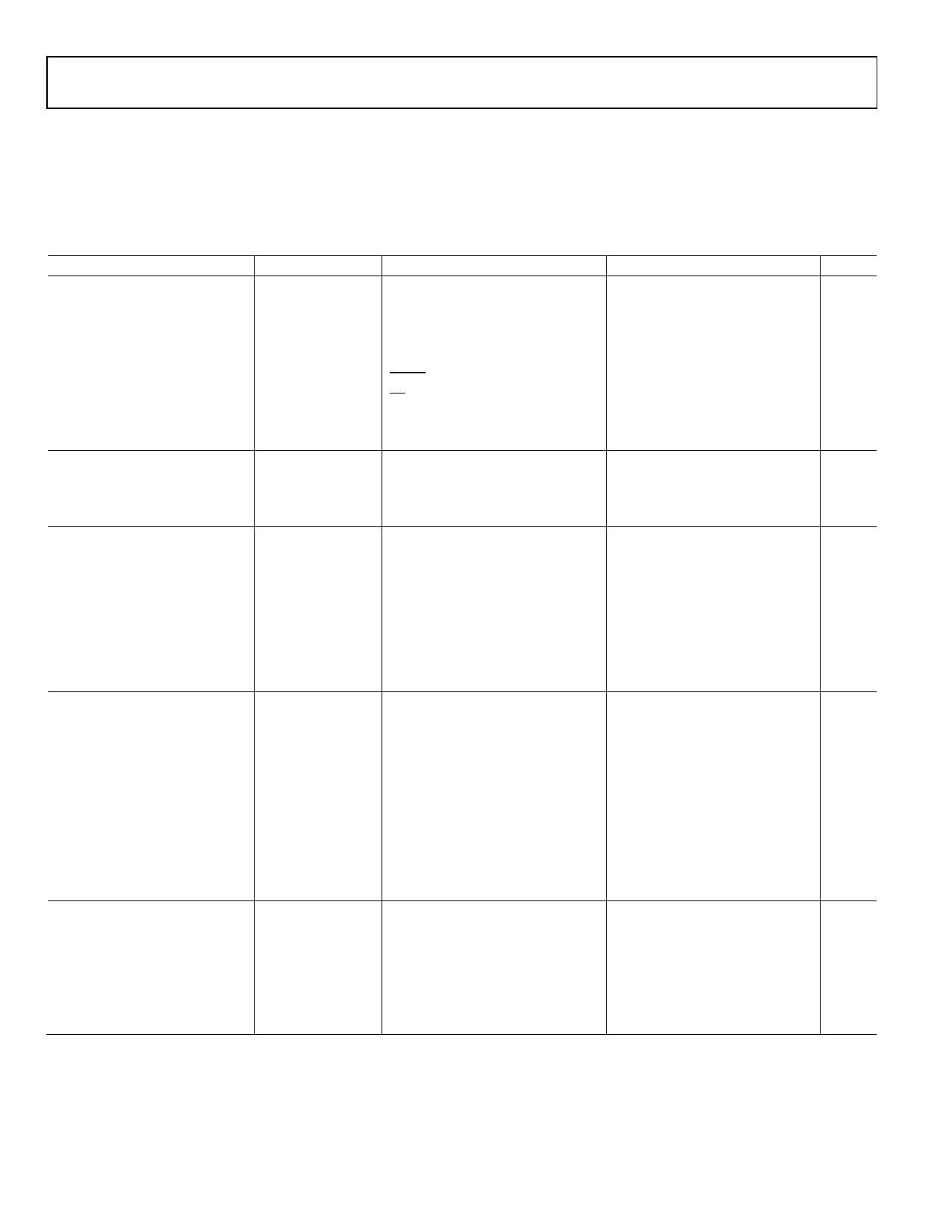
Table 1.
Parameter
DIGITAL INPUTS1
Input High Voltage
Input Low Voltage
Input Current
Symbol
VIH
VIH
VIL
VIL
IIN
Input Capacitance
CIN
DIGITAL INPUTS (5 V TOLERANT)1, 2
Input High Voltage
VIH
Input Low Voltage
VIL
Input Current
IIN
DIGITAL OUTPUTS1
Output High Voltage
VOH
Output Low Voltage
VOL
High Impedance Leakage
ILEAK
Current
Output Capacitance
POWER REQUIREMENTS3,4
Digital Core Power Supply
Digital I/O Power Supply
PLL Power Supply
Terminator Power Supply
Comparator Power Supply
Digital Core Supply Current
Digital I/O Supply Current
PLL Supply Current
Terminator Supply Current
Comparator Supply Current
POWER-DOWN CURRENTS3,6
Digital Core Supply Current
Digital I/O Supply Current
PLL Supply Current
Terminator Supply Current
Comparator Supply Current
Power-Up Time
COUT
DVDD
DVDDIO
PVDD
TVDD
CVDD
IDVDD
IDVDDIO
IPVDD
ITVDD
ICVDD
IDVDD_PD
IDVDDIO_PD
IPVDD_PD
ITVDD_PD
ICVDD_PD
tPWRUP
Test Conditions/Comments
Min
XTALN and XTALP
1.2
Other digital inputs
2
XTALN and XTALP
Other digital inputs
RESET pin
CS pin
Other digital inputs
2.6
−82
2.4
VS/FIELD/ALSB pin
HPA_A/INT2, HPA_B pin
Digital inputs other than XTALN
and XTALP
1.71
3.14
1.71
3.14
1.71
Dual 1080p60 12 bit with BG5port
Dual 1080p60 12 bit with BG5 port
Dual 1080p60 12 bit with BG5 port
Dual 1080p60 12 bit with BG5 port
Dual 1080p60 12 bit with BG5 port
Typ
±45
±45
±10
±35
±10
1.8
3.3
1.8
3.3
1.8
149.5
9.9
36.9
121.4
187.0
0.3
1.3
1.5
0.1
1.3
25
Max
Unit
V
V
0.4
V
0.8
V
±60
µA
±60
µA
µA
10
pF
V
0.8
V
+82
µA
V
0.4
V
±60
µA
±82
µA
µA
20
pF
1.89
V
3.46
V
1.89
V
3.46
V
1.89
V
201.9
mA
178.5
mA
39.2
mA
134.5
mA
210.9
mA
0.4
mA
1.7
mA
1.8
mA
0.3
mA
1.7
mA
ms
1 Data guaranteed by characterization.
2 The following pins are 5 V tolerant: DDCA_SCL, DDCA_SDA, DDCB_SCL, DDCB_SDA, RXA_5V, and RXB_5V.
3 Data recorded during lab characterization
4 Maximum current consumption values are recorded with maximum rated voltage supply levels, MoireX video pattern, and at maximum rated temperature.
5 BG = background.
6 Power-Down Mode 0 (IO map, Register 0x0C = 0x62), ring oscillator powered down (HDMI map, Register 0x48 = 0x01), and DDC pads off (HDMI map, Register 0x73 = 0x03).
Rev. E | Page 4 of 20
Share Link: 