MC74HC151ADG Просмотр технического описания (PDF) - ON Semiconductor
Номер в каталоге
Компоненты Описание
Список матч
MC74HC151ADG Datasheet PDF : 7 Pages
| |||
MC74HC151A
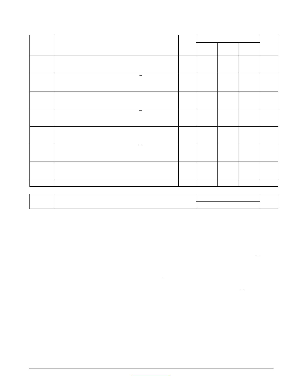
AC ELECTRICAL CHARACTERISTICS (CL = 50 pF, Input tr = tf = 6 ns)
Symbol
tPLH,
tPHL
Parameter
Maximum Propagation Delay, Input D to Output Y
(Figures 2 and 7)
tPLH,
tPHL
Maximum Propagation Delay, Input D to Output Y
(Figures 4 and 7)
tPLH,
tPHL
Maximum Propagation Delay, Input D to Output Y
(Figures 3 and 7)
tPLH,
tPHL
Maximum Propagation Delay, Input A to Output Y
(Figures 3 and 7)
tPLH,
tPHL
Maximum Propagation Delay, Input D to Output Y
(Figures 5 and 7)
tPLH,
tPHL
Maximum Propagation Delay, Strobe to Output Y
(Figures 6 and 7)
tTLH,
tTHL
Maximum Output Transition Time, Any Output
(Figures 2, 4 and 7)
Cin
Maximum Input Capacitance
CPD
Power Dissipation Capacitance (Per Package)
Guaranteed Limit
VCC
− 55 to
V
25°C
v 85°C v 125°C Unit
2.0
170
215
255
ns
4.5
34
43
51
6.0
29
37
43
2.0
185
230
280
ns
4.5
37
46
56
6.0
31
39
48
2.0
185
230
280
ns
4.5
37
46
56
6.0
31
39
48
2.0
205
255
310
ns
4.5
41
51
62
6.0
35
43
53
2.0
125
155
190
ns
4.5
25
31
38
6.0
21
26
32
2.0
125
155
190
ns
4.5
25
31
38
6.0
21
26
32
2.0
75
4.5
15
6.0
13
95
110
ns
19
22
16
19
−
10
10
10
pF
Typical @ 25°C, VCC = 5.0 V
36
pF
PIN DESCRIPTIONS
INPUTS
D0, D1, … , D7 (Pins 4, 3, 2, 1, 15, 14, 13, 12)
Data inputs. Data on any one of these eight binary inputs
may be selected to appear on the output.
CONTROL INPUTS
A0, A1, A2 (Pins 11, 10, 9)
Address inputs. The data on these pins are the binary
address of the selected input (see the Function Table).
Strobe (Pin 7)
Strobe. This input pin must be at a low level for the
selected data to appear at the outputs. If the Strobe pin is
high, the Y output is forced to a low level and the Y output
is forced to a high level.
OUTPUTS
Y, Y (Pins 5, 6)
Data outputs. The selected data is presented at these pins
in both true (Y output) and complemented (Y output) forms.
www.onsemi.com
3
Share Link: 