TC7MPN3245FTG(2007) Просмотр технического описания (PDF) - Toshiba
Номер в каталоге
Компоненты Описание
Список матч
TC7MPN3245FTG Datasheet PDF : 22 Pages
| |||

TC7MPN3245FTG
TOSHIBA Digital Integrated Circuit Silicon Monolithic
TC7MPN3245FTG
Low Voltage/Low Power 4-Bit × 2 Dual Supply Bus Transceiver
The TC7MPN3245FTG is an advanced high-speed CMOS 8-bit
dual supply voltage interface bus transceiver, fabricated with silicon
gate CMOS technology.
It is also designed with over-voltage tolerant inputs and outputs up
to 3.6 V.
Designed for use as an interface between a 1.2-V, 1.5-V, 1.8-V, or
2.5-V bus and a 1.8-V, 2.5-V or 3.6-V bus in mixed 1.2-V, 1.5-V,
1.8-V or 2.5-V/1.8-V, 2.5-V or 3.6-V supply systems.
The A-port interfaces with the 1.2-V, 1.5-V, 1.8-V or 2.5-V bus, the
B-port with the 1.8-V, 2.5-V, 3.3-V bus.
The direction of data transmission is determined by the level of the
Weight: 0.03 g (typ.)
DIR input. The enable input ( OE ) can be used to disable the device
so that the buses are effectively isolated.
All inputs are equipped with protection circuits against static discharge or transient excess voltage.
Features
• Bidirectional interface between 1.2-V and 1.8-V, 1.2-V and 2.5-V, 1.2-V and 3.3-V, 1.5-V and 2.5-V, 1.5-V and 3.3-V,
1.8-V and 2.5-V, 1.8-V and 3.3-V or 2.5-V and 3.3-V buses.
• High-speed operation : tpd = 13.7 ns (max) (VCCA = 2.5 ± 0.2 V, VCCB = 3.3 ± 0.3 V)
tpd = 14.8 ns (max) (VCCA = 1.8 ± 0.15 V, VCCB = 3.3 ± 0.3 V)
tpd = 16.0 ns (max) (VCCA = 1.5 ± 0.1 V, VCCB = 3.3 ± 0.3 V)
tpd = 61 ns (max) (VCCA = 1.2 ± 0.1 V, VCCB = 3.3 ± 0.3 V)
tpd = 18.5 ns (max) (VCCA = 1.8 ± 0.15 V, VCCB = 2.5 ± 0.2 V)
tpd = 19.7 ns (max) (VCCA = 1.5 ± 0.1 V, VCCB = 2.5 ± 0.2 V)
tpd = 60 ns (max) (VCCA = 1.2 ± 0.1 V, VCCB = 2.5 ± 0.2 V)
tpd = 58 ns (max) (VCCA = 1.2 ± 0.1 V, VCCB = 1.5 ± 0.1 V)
• Output current : IOHB/IOLB = ±3 mA (min) (VCCB = 3.0 V)
IOHB/IOLB = ±2 mA (min) (VCCB = 2.3 V)
IOHB/IOLB = ±0.5 mA (min) (VCCB = 1.65 V)
IOHA/IOLA = ±9 mA (min) (VCCA = 2.3 V)
IOHA/IOLA = ±3 mA (min) (VCCA = 1.65 V)
IOHA/IOLA = ±1 mA (min) (VCCA = 1.4 V)
• Latch-up performance: ±300 mA
• ESD performance: Machine model ≥ ±200 V
Human body model ≥ ±2000 V
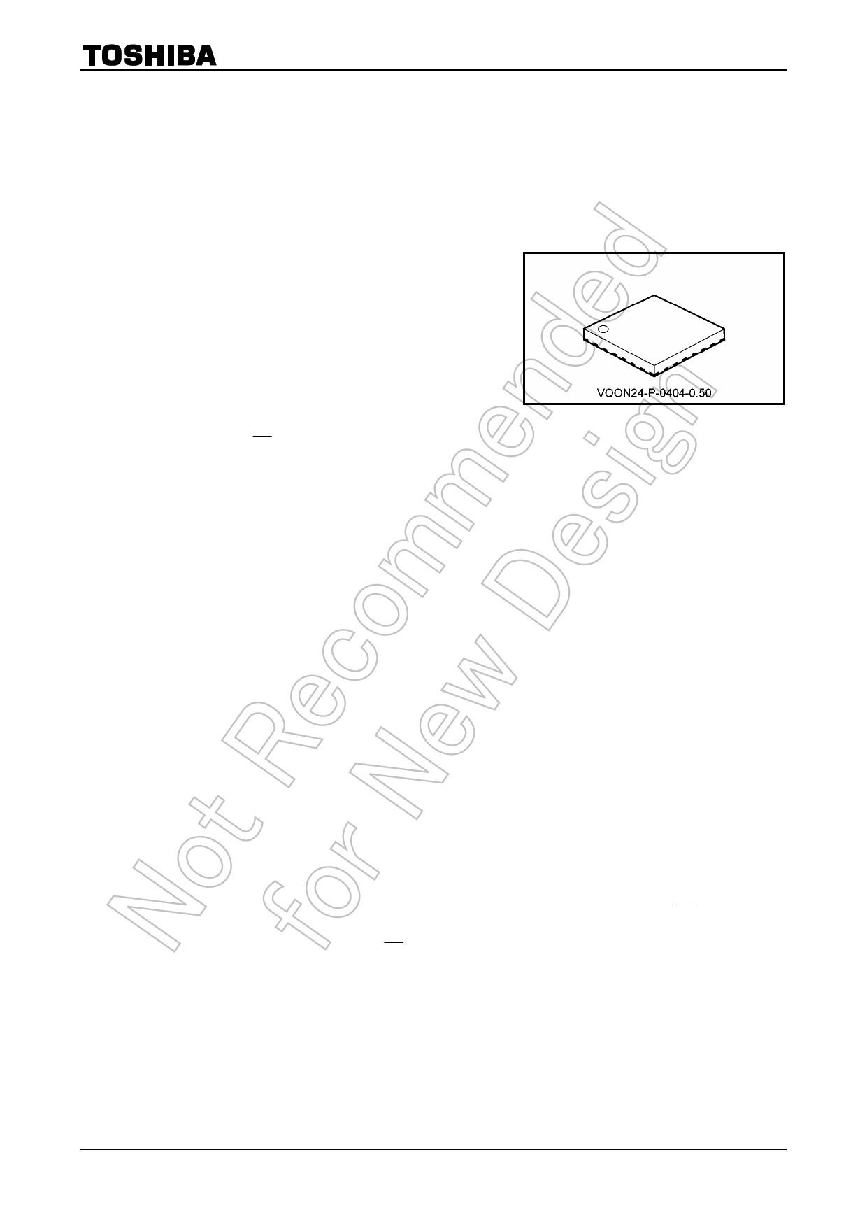
• Ultra-small package: VQON24
• Low current consumption : Using the new circuit significantly reduces current consumption when OE = “H”.
Suitable for battery-driven applications such as PDAs and cellular phones.
• Floating A-bus and B-bus are permitted. (when OE = “H”)
3.6-V tolerant function and power-down protection provided on all inputs and outputs.
Note 1: Do not apply a signal to any bus pin when it is in the output mode. Damage may result.
Note 2: RA or RMA flux is recommended when mounting the VQON package.
1
2007-10-19