HD61830 Просмотр технического описания (PDF) - Hitachi -> Renesas Electronics
Номер в каталоге
Компоненты Описание
Список матч
HD61830 Datasheet PDF : 43 Pages
| |||
HD61830/HD61830B
Display Control Instructions
Display is controlled by writing data into the instruction register and 13 data registers. The RS signal
distinguishes the instruction register from the data registers. 8-bit data is written into the instruction register
with RS = 1, and the data register code is specified. After that, the 8-bit data is written in the data register
and the specified instruction is executed with RS = 0.
During the execution of the instruction, no new instruction can be accepted. Since the busy flag is set
during this, read the busy flag and make sure it is 0 before writing the next instruction.
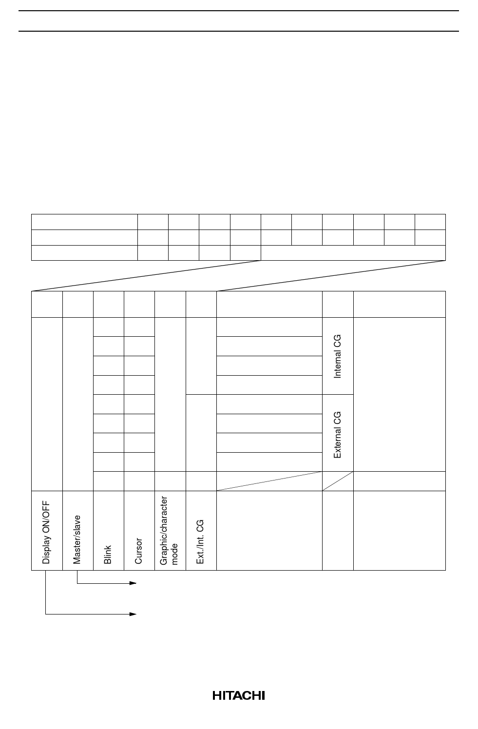
1. Mode Control: (Execution time: 4 µs) Code H'00 (hexadecimal) written into the instruction register
specifies the mode control register.
Register
Instruction reg.
Mode control reg.
R/W RS DB7 DB6 DB5 DB4 DB3 DB2 DB1 DB0
0
1
0
0
0
0
0
0
0
0
0
0
0
0
Mode data
DB5 DB4 DB3 DB2 DB1 DB0
Cursor/blink
1/0 1/0
0
0
0
0 Cursor off
0
1
Cursor on
Graphic/character
CG
display
Character display
(Character mode)
1
0
Cursor off, character blink
1
1
Cursor blink
0
0
1 Cursor off
0
1
Cursor on
1
0
Cursor off, character blink
1
1
Cursor blink
0
0
1
0
Graphic mode
1: Master mode
0: Slave mode
1: Display ON
0: Display OFF
9
Share Link: 