G952T43U Просмотр технического описания (PDF) - Global Mixed-mode Technology Inc
Номер в каталоге
Компоненты Описание
Список матч
G952T43U Datasheet PDF : 11 Pages
| |||
Global Mixed-mode Technology Inc.
G952
Absolute Maximum Ratings (Note 1)
Input Voltage . . . . . . . . . . . . . . . . . . . . . . . . . . . . 7V
Power Dissipation Internally Limited
(Note 2)
Maximum Junction Temperature . . . . . . . . . . . 150°C
Storage Temperature
Range . . . . . . . . . . . . . . . . . . . . .65°C ≤ TJ ≤+150°C
Reflow Temperature (soldering, 10sec) . . . . . 260°C
Thermal Resistance Junction to Ambient, (θJA)
SOT-89 . . . . . . . . . . . . . . . . . . . . . . . . . . . .173°C/W
SOT-223 . . . . . . . . . . . . . . . . . . . . . . . . . . .148°C/W
TO-252 . . . . . . . . . . . . . . . . . . . . . . . . . . . .124°C/W
Thermal Resistance Junction to Case, (θJc)
SOT-89. . . . . . . . . . . . . . . . . . . . . . . . . . . . . 25°C/W
SOT-223. . . . . . . . . . . . . . . . . . . . . . . . . . . 22°C/W
TO-252. . . . . . . . . . . . . . . . . . . . . . . . . . . . . .7°C/W
Operating Conditions
(Note 1)
Input Voltage . . . . . . . . . . . . . . . . . . . . . . . . .2.7V~6.5V
Temperature Range. . . . . . . . . . . . . . -40°C ≤ TA ≤85°C
Note (1): See Recommended Minimum Footprint
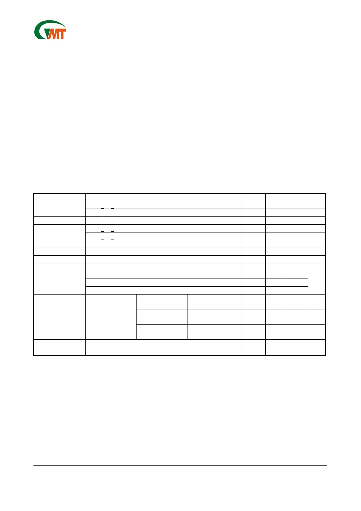
Electrical Characteristics
VIN =3.3V, IO = 1A, CIN = 1µF, COUT =10µF, All specifications apply for TA = TJ = 25°C. [Note 3]
PARAMETER
CONDITION
Output Voltage
10mA < IO < 1A
10mA < IO < 550mA (SOT-89)
Line Regulation
3V < VIN < 6.5V, IO = 10mA
Load Regulation
10mA < IO < 1A
10mA < IO < 550mA (SOT-89)
Output Impedance 200mA DC and 100mA AC, fo = 120Hz
Quiescent Current VIN = 3.3V
Ripple Rejection
fi = 120Hz,Vripple =1VP-P, Io = 100mA
IO = 0A
Dropout Voltage
IO = 100mA
IO = 500mA for (SOT-89,SOT-223,TO-252)
IO = 1A only for (SOT-223,TO-252)
Output Current
Minimum footprint
VIN = 3V(SOT-223) (0.0625 square inch)
Continuous Test,
TA = 25°C, TJ 150°C,
VOUT within ±2%
VIN = 3.3V(SOT-223)
Mounted on 0.53
square inch pcb area
Mounted on 0.16
VIN = 3.3V(SOT-89) square inch pcb area
Short Circuit Current
Over Temperature
MIN
1.764
1.764
---
---
---
---
300
---
---
---
---
---
---
TYP
1.800
1.800
3
30
30
80
480
53
880
895
950
1160
660
---
1
---
0.5
---
1.6
---
150
MAX
1.845
1.845
30
50
50
---
1500
---
---
---
---
---
UNIT
V
V
mV
mV
mV
mΩ
µA
dB
mV
--- mA
---
A
---
A
---
A
---
°C
Note 1:
Note2:
Note3:
Note4:
Absolute Maximum Ratings are limits beyond which damage to the device may occur. Operating Conditions are
conditions under which the device functions but the specifications might not be guaranteed. For guaranteed specifications
and test conditions see the Electrical Characteristics.
The maximum power dissipation is a function of the maximum junction temperature, TJmax ; total thermal resistance, θJA,
and ambient temperature TA. The maximum allowable power dissipation at any ambient temperature is Tjmax-TA / θJA. If
this dissipation is exceeded, the die temperature will rise above 150°C and IC will go into thermal shutdown. For the
G952 in SOT-89 package. θJA is 173°C/W For the G952 in SOT-223 package, θJA is 148°C/W, in TO-252 package, θJA
is 124°C/W. (See recommend minimum footprint). The safe operation in SOT- 89, SOT-223, TO-252 package, it can
see “Typical Performance Characteristics” (Safe Operating Area).
Low duty pulse techniques are used during test to maintain junction temperature as close to ambient as possible.
The type of output capacitor should be tantalum or aluminum.
Ver: 2.6
Mar 19, 2007
TEL: 886-3-5788833
http://www.gmt.com.tw
2
Share Link: 