LC8220 Просмотр технического описания (PDF) - SANYO -> Panasonic
Номер в каталоге
Компоненты Описание
Список матч
LC8220 Datasheet PDF : 13 Pages
| |||
LC8220
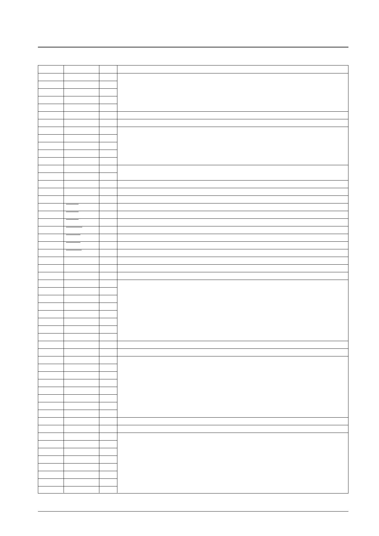
Continued from preceding page.
Pin No.
55
56
57
58
59
60
61
62
63
64
65
66
67
68
69
70
71
72
73
74
75
76
77
78
79
80
81
82
83
84
85
86
87
88
89
90
91
92
93
94
95
96
97
98
99
100
101
102
103
104
105
106
107
108
109
Symbol
MDD4
MDD3
MDD2
MDD1
MDD0
VDD
VSS
TESTI1
TESTI2
TESTI3
TESTI4
TESTI5
TESTO1
TESTO2
TESTI6
TESTO3
CPUPX
PXCS
PXRD
PXWR
PXRDY
PXINT
PXRLS
PXEND
(NC)
VDD
VSS
PXD31
PXD30
PXD29
PXD28
PXD27
PXD26
PXD25
PXD24
VDD
VSS
PXD23
PXD22
PXD21
PXD20
PXD19
PXD18
PXD17
PXD16
VDD
VSS
PXD15
PXD14
PXD13
PXD12
PXD11
PXD10
PXD9
PXD8
I/O
Function
I/O
I/O
I/O Test mode data bus*7
I/O
I/O
— +5 V power supply
— Ground
I
I
I Test mode input pins*9
I
I
O
Test mode output pins*8
O
I Test mode input pin*9
O Test mode output pin*8
I Connected CPU type setting for the pixel bus*1
I Pixel bus chip select*2
I Pixel bus read request*3
I Pixel bus write request*4
O Pixel bus ready for read/write requests*5
O Pixel bus interrupt request
I Pixel bus interrupt release
O Pixel bus last data output indicator
—
— +5 V power supply
— Ground
I/O
I/O
I/O
I/O Pixel data bus
I/O (D31 to D16 are unused if a 16-bit CPU is used and D31 to D8 are unused if an 8-bit CPU is used.*7)
I/O
I/O
I/O
— +5 V power supply
— Ground
I/O
I/O
I/O
I/O Pixel data bus
I/O (D31 to D16 are unused if a 16-bit CPU is used and D31 to D8 are unused if an 8-bit CPU is used.*7)
I/O
I/O
I/O
— +5 V power supply
— Ground
I/O
I/O
I/O
I/O Pixel data bus
I/O (D31 to D16 are unused if a 16-bit CPU is used and D31 to D8 are unused if an 8-bit CPU is used.*7)
I/O
I/O
I/O
Continued on next page.
No. 4909-4/13
Share Link: 