LTC1535 Просмотр технического описания (PDF) - Linear Technology
Номер в каталоге
Компоненты Описание
Список матч
LTC1535 Datasheet PDF : 18 Pages
| |||
LTC1535
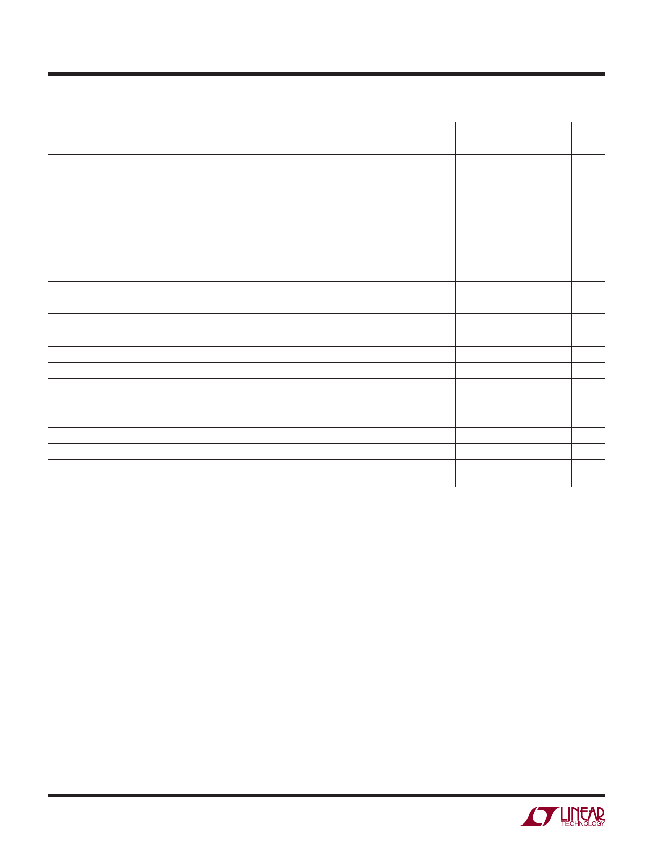
ELECTRICAL CHARACTERISTICS The l denotes the specifications which apply over the full operating
temperature range, otherwise specifications are at TA = 25°C. VCC = 5V, VCC2 = 5V, R = 27Ω (RS485) unless otherwise noted.
SYMBOL PARAMETER
CONDITIONS
MIN TYP MAX UNITS
tSJ
fMAX
tPLH
tPHL
tr, tf
tZH
tZL
tLZ
tHZ
tPLH
tPHL
tPLH
tPHL
tr, tf
tLZ
tHZ
tSTART
Data Sample Jitter
Max Baud Rate
Driver Input to Output
Driver Input to Output
Driver Rise or Fall Time
Driver Enable to Output
Driver Enable to Output
Driver Disable to Output
Driver Disable to Output
Receiver Input to RO
Receiver Input to RO
Receiver Input to RO2
Receiver Input to RO2
Receiver Rise or Fall Time
Receiver Disable to Output
Receiver Disable to Output
Initial Start-Up Time
Figure 8, (Note 7)
Jitter = 10% Max, SLO = 1, (Note 8)
DE = 1, SLO = 1, Figure 4, Figure 6
DE = 1, SLO = 0, Figure 4, Figure 6
DE = 1, SLO = 1, Figure 4, Figure 6
DE = 1, SLO = 1, Figure 4, Figure 6
DE = 1, SLO = 1, Figure 4, Figure 6
DE = 1, SLO = 0, VCC = VCC2 = 4.5V
DI = 1, SLO = 1, Figure 5, Figure 7
DI = 0, SLO = 1, Figure 5, Figure 7
DI = 0, SLO = 1, Figure 5, Figure 7
DI = 1, SLO = 1, Figure 5, Figure 7
RE = 0, Figure 3, Figure 8
RE = 0, Figure 3, Figure 8
RE = 0, Figure 3, Figure 8
RE = 0, Figure 3, Figure 8
RE = 0, Figure 3, Figure 8
Figure 3, Figure 9
Figure 3, Figure 9
(Note 9)
l
250
285
ns
l 250
410
kBd
l
600
855
ns
l
1300 1560
ns
l
600
855
ns
l
1300 1560
ns
l
20
100
ns
l 150
500 1000
ns
l
1000 1400
ns
l
1000 1400
ns
l
700 1300
ns
l
700 1300
ns
l
600
855
ns
l
600
855
ns
30
ns
30
ns
20
ns
30
ns
30
ns
1200
ns
tTOF
Data Time-Out Fault
ST1, ST2 Duty Cycle
(Note 9)
0°C ≤ TA ≤ 70°C
–40°C ≤ TA ≤ 85°C
1200
ns
l
56
%
l
57
%
Note 1: Absolute Maximum Ratings are those values beyond which the life
of a device may be impaired.
Note 2: RS422 50Ω specification based on RS485 27Ω test.
Note 3: IIN is tested at VCC2 = 5V, guaranteed by design from
GND2 ≤ VCC2 ≤ 5.25V.
Note 4: Input fault conditions on the RS485 receiver are detected with a
fixed receiver offset. The offset is such that an input short or open will
result in a high data output.
Note 5: The low voltage detect faults when VCC2 or VCC drops below
VUVL and reenables when greater than VUVH. The fault can be monitored
through the weak driver output on RE.
Note 6: Value derived from 1 second test.
Note 7: The input signals are internally sampled and encoded. The internal
sample rate determines the data output jitter since the internal sampling is
asynchronous with respect to the external data. Nominally, a 4MHz internal
sample rate gives 250ns of sampling uncertainty in the input signals.
Note 8: The maximum baud rate is 250kBd with 10% sampling jitter.
Lower baud rates have lower jitter.
Note 9: Start-up time is the time for communication to recover after a fault
condition. Data time-out is the time a fault is indicated on RE after data
communication has stopped.
Note 10: ICC measured with no load, ST1 and ST2 floating.
1535fb
4
Share Link: 