LTC1535(1999) Просмотр технического описания (PDF) - Linear Technology
Номер в каталоге
Компоненты Описание
Список матч
LTC1535 Datasheet PDF : 12 Pages
| |||
LTC1535
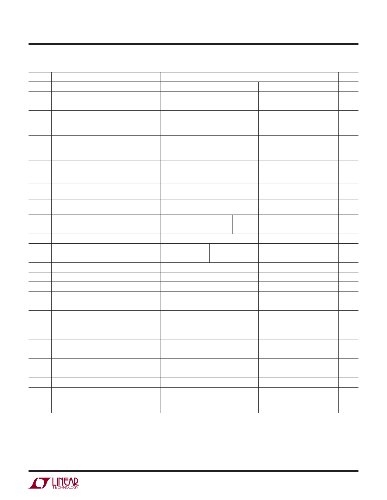
ELECTRICAL CHARACTERISTICS The q denotes the specifications which apply over the full operating
temperature range, otherwise specifications are at TA = 25°C. 0°C ≤ TA ≤ 70°C, VCC = 5V, VCC2 = 5V unless otherwise noted.
SYMBOL
IOZ
VOH2
VOL2
fSW
RSWH
RSWL
IREL
IREH
VUVL
VUVH
VISO
PARAMETER
Driver Output Leakage
RO2 Output High Voltage
RO2 Output Low Voltage
DC Converter Frequency
DC Converter R High
DC Converter R Low
RE Output Low Current
RE Output High Current
Undervoltage Low Threshold
Undervoltage High Threshold
Isolation Voltage
CONDITIONS
IRO2 = – 4mA, VCC = 4.5V
IRO2 = –10mA, VCC = 4.5V
IRO2 = 4mA, VCC = 4.5V
IRO2 = 10mA, VCC = 4.5V
VCC = 4.5V
VCC = 4.5V
RE Sink Current, Fault = 0
RE Source Current, Fault = 1
RE Fault = 1, Note 5
RE Fault = 0, Note 5
1 Minute, Note 6
1 Second
MIN TYP MAX UNITS
1
µA
q 3.7
3.9
V
3.4
V
q
0.4
0.8
V
0.9
V
q 290
420
520
kHz
q
4
6
Ω
q
2.5
5
Ω
q – 40 – 50 – 80
µA
q 80
100 130
µA
q 3.90 4.00 4.25
V
q 4.05 4.20 4.40
V
2500
3000
VRMS
VRMS
U
SWITCHI G CHARACTERISTICS The q denotes the specifications which apply over the full operating
temperature range, otherwise specifications are at TA = 25°C. 0°C ≤ TA ≤ 70°C, VCC = 5V, VCC2 = 5V, R = 27Ω (RS485) unless
otherwise noted.
SYMBOL
tSJ
fMAX
tPLH
tPHL
tr, tf
tZH
tZL
tLZ
tHZ
tPLH
tPHL
tPLH
tPHL
tr, tf
tLZ
tHZ
tSTART
tTOF
PARAMETER
Data Sample Jitter
Max Baud Rate
Driver Input to Output
Driver Input to Output
Driver Rise or Fall Time
Driver Enable to Output
Driver Enable to Output
Driver Disable to Output
Driver Disable to Output
Receiver Input to RO
Receiver Input to RO
Receiver Input to RO2
Receiver Input to RO2
Receiver Rise or Fall Time
Receiver Disable to Output
Receiver Disable to Output
Initial Start-Up Time
Data Time-Out Fault
CONDITIONS
Figure 8, Note 7
Jitter = 10% Max, SLO = 1, Note 8
DE = 1, SLO = 1, Figure 3, Figure 5
DE = 1, SLO = 0, Figure 3, Figure 5
DE = 1, SLO = 1, Figure 3, Figure 5
DE = 1, SLO = 0, Figure 3, Figure 5
DE = 1, SLO = 1, Figure 3, Figure 5
DE = 1, SLO = 0
DI = 1, SLO = 1, Figure 4, Figure 6
DI = 0, SLO = 1, Figure 4, Figure 6
DI = 0, SLO = 1, Figure 4, Figure 6
DI = 1, SLO = 1, Figure 4, Figure 6
RE = 0, Figure 2, Figure 7
RE = 0, Figure 2, Figure 7
RE = 0, Figure 2, Figure 7
RE = 0, Figure 2, Figure 7
RE = 0, Figure 2, Figure 7
Figure 2, Figure 8
Figure 2, Figure 8
Note 9
Note 9
MIN TYP MAX UNITS
q
250 285
ns
q 350
kBd
q
600 855
ns
q
1300 1560
ns
q
600 855
ns
q
1300 1560
ns
q
20
50
ns
q 150
500 1000
ns
q
1000 1400
ns
q
1000 1400
ns
q
700 1000
ns
q
700 1000
ns
q
600 855
ns
q
600 855
ns
30
ns
30
ns
20
ns
30
ns
30
ns
1200
ns
1200
ns
3
Share Link: 