A28F010 Просмотр технического описания (PDF) - Intel
Номер в каталоге
Компоненты Описание
Список матч
A28F010 Datasheet PDF : 23 Pages
| |||
A28F010
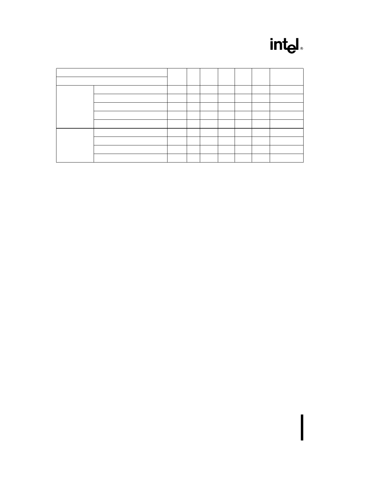
Table 2 28F010 Bus Operations
Operation
Pins VPP(1) A0 A9 CE OE WE
DQ0 – DQ7
Read
VPPL A0 A9 VIL VIL VIH Data Out
Output Disable
VPPL X
X
VIL VIH VIH Tri-State
READ-ONLY Standby
Intelligent Identifier (Mfr)(2)
VPPL X
X
VIH
X
X Tri-State
VPPL VIL VID(3) VIL VIL VIH Data e 89H
Intelligent Identifier (Device)(2) VPPL VIH VID(3) VIL VIL VIH Data e B4H
Read
VPPH A0 A9 VIL VIL VIH Data Out(4)
READ WRITE Output Disable
Standby(5)
VPPH X
X
VIL VIH VIH Tri-State
VPPH X
X
VIH
X
X Tri-State
Write
VPPH A0 A9 VIL VIH VIL Data In(6)
NOTES
1 VPPL may be ground a no-connect with a resistor tied to ground or s 6 5V VPPH is the programming voltage specified
for the device Refer to D C Characteristics When VPP e VPPL memory contents can be read but not written or erased
2 Manufacturer and device codes may also be accessed via a command register write sequence Refer to Table 3 All other
addresses low
3 VID is the Intelligent Identifier high voltage Refer to DC Characteristics
4 Read operations with VPP e VPPH may access array data or the Intelligent Identifier codes
5 With VPP at high voltage the standby current equals ICC a IPP (standby)
6 Refer to Table 3 for valid Data-In during a write operation
7 X can be VIL or VIH
the contents of the register default to the read com-
mand making the 28F010 a read-only memory
Memory contents cannot be altered
Or the system designer may choose to ‘‘hardwire’’
VPP making the high voltage supply constantly
available In this instance all operations are per-
formed in conjunction with the command register
The 28F010 is designed to accommodate either de-
sign practice and to encourage optimization of the
processor-memory interface
The two-step Program Erase write sequence to the
Command Register provides additional software
write protection
BUS OPERATIONS
Read
The 28F010 has two control functions both of which
must be logically active to obtain data at the out-
puts Chip-Enable (CE ) is the power control and
should be used for device selection Output-Enable
(OE ) is the output control and should be used to
gate data from the output pins independent of de-
vice selection Figure 6 illustrates read timing wave-
forms
When VPP is low (VPPL) the read only operation is
active This permits reading the data in the array and
outputting the Intelligent Identifier codes (see Ta-
ble 2) When VPP is high (VPPH) the default condi-
tion of the device is the read only mode This allows
reading the data in the array Further functionality is
achieved though the Command Register as shown
in Table 3
Output Disable
With Output-Enable at a logic-high level (VIH) output
from the device is disabled Output pins are placed
in a high-impedance state
Standby
With Chip-Enable at a logic-high level the standby
operation disables most of the 28F010’s circuitry
and substantially reduces device power consump-
tion The outputs are placed in a high-impedance
state independent of the Output-Enable signal If
the 28F010 is deselected during erasure program-
ming or program erase verification the device
draws active current until the operation is terminat-
ed
Intelligent Identifier Operation
The Intelligent Identifier operation outputs the manu-
facturer code (89H) and device code (B4H) Pro-
gramming equipment automatically matches the
device with its proper erase and programming
algorithms
6
Share Link: 