HM1-6518B-9 Просмотр технического описания (PDF) - Intersil
Номер в каталоге
Компоненты Описание
Список матч
HM1-6518B-9 Datasheet PDF : 7 Pages
| |||
HM-6518
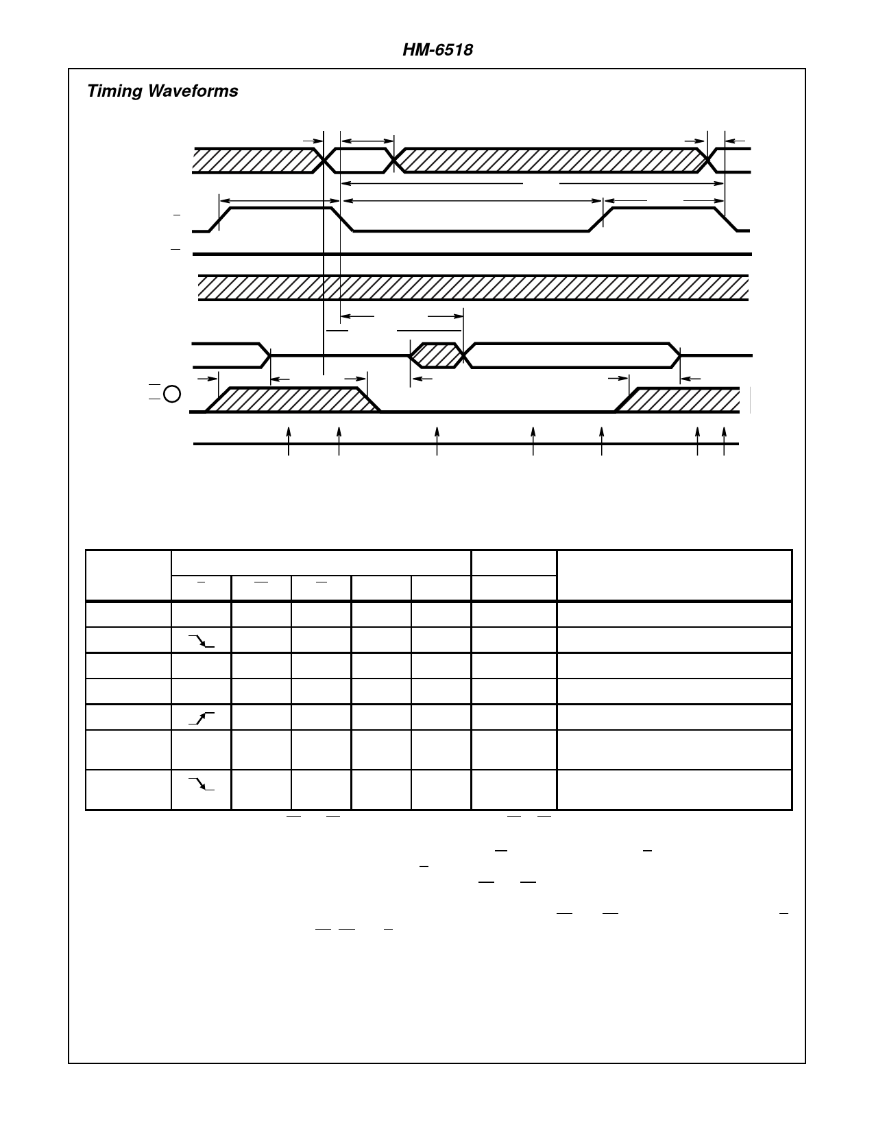
Timing Waveforms
(8)
TAVEL
A
TEHEL
E
(7)
HIGH
W
(9)
TELAX
VALID
TELEH
(6)
TELEL
(8)
TAVEL
TEHEL
(7)
NEXT
(17)
D
Q
S1, 1
S2
PREVIOUS
DATA
TSHQZ
HIGH Z
(5)
TELQV (1)
TAVQV (2)
TSLOX
(3)
VALID OUTPUT LATCHED
(5)
TSHQZ
HIGH Z
TIME
REFERENCE
-1
0
1
2
3
45
FIGURE 1. READ CYCLE
TRUTH TABLE
TIME
REFERENCE
E
INPUTS
S1
W
A
OUTPUTS
D
Q
FUNCTION
-1
H
H
X
X
X
Z
Memory Disabled
0
X
H
V
X
Z
Cycle Begins, Addresses are Latched
1
L
L
H
X
X
X
Output Enabled
2
L
L
H
X
X
V
Output Valid
3
L
H
X
X
V
Output Latched
4
H
H
X
X
X
Z
Device Disabled, Prepare for Next Cycle
(Same as -1)
5
X
H
V
X
Z
Cycle Ends, Next Cycle Begins
(Same as 0)
NOTE: 1. Device selected only if both S1 and S2 are low, and deselected if either S1 or S2 are high.
In the HM-6518 read cycle the address information is
latched into the on chip registers on the falling edge of E
(T = 0). Minimum address setup and hold time require-
ments must be met. After the required hold time the
addresses may change state without affecting device oper-
ation. In order for the output to be read S1, S2 and E must
be low, W must be high. When E goes high, the output
data is latched into an on chip register. Taking either or
both S1 or S2 high, forces the output buffer to a high
impedance state. The output data may be re-enabled at
any time by taking S1 and S2 low. On the falling edge of E
the data will be unlatched.
6-5
Share Link: 