AD537SD/883B Просмотр технического описания (PDF) - Analog Devices
Номер в каталоге
Компоненты Описание
Список матч
AD537SD/883B Datasheet PDF : 8 Pages
| |||
AD537
NONLINEARITY SPECIFICATION
The preferred method for specifying linearity error is in terms of
the maximum deviation from the ideal relationship after cali-
brating the converter at full scale and “zero”. This error will
vary with the full-scale frequency and the mode of operation.
The AD537 operates best at a 10 kHz full-scale frequency with
a negative voltage input; the linearity is typically within ± 0.05%.
Operating at higher frequencies or with positive inputs will
degrade the linearity as indicates in the Specification table. The
shape of a typical linearity plot is given in Figure 4.
0.18
0.16 TEST CONDITIONS:
0.14
+VS = +15V
–VS = 0V
0.12 CT = 0.01µF
0.10
RT = 10kΩ
VFS = ±10V
0.08 POS INPUT – FIG. 3
NEG INPUT – FIG. 4
0.06
AD537J
0.04
0.02
0
–0.02
–0.04
AD537K, S
–0.06
–0.08
1
10
100
1k
10k
OUTPUT FREQUENCY – Hz
Figure 4a. Typical Nonlinearity Error Envelopes with
10 kHz F.S. Output
0.18
0.16 TEST CONDITIONS:
0.14
+VS = +15V
–VS = 0V
0.12 CT = 0.001µF
0.10
RT = 10kΩ
VFS = ±10V
0.08 POS INPUT – FIG. 3
NEG INPUT – FIG. 4
0.06
AD537J
0.04
0.02
0
–0.02
AD537K, S
–0.04
–0.06
–0.08
10
100
1k
10k
OUTPUT FREQUENCY – Hz
100k
Figure 4b. Typical Nonlinearity Error with 100 kHz F.S.
Output
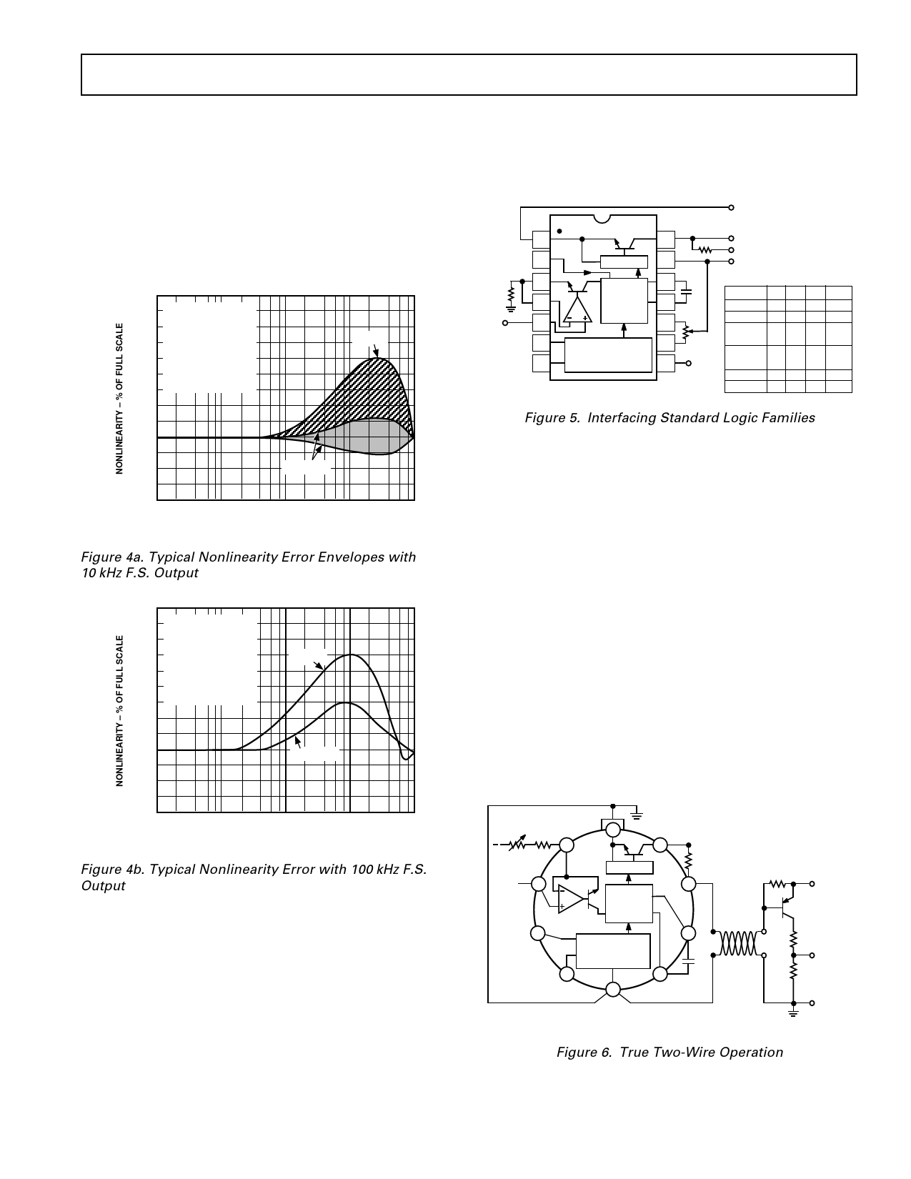
OUTPUT INTERFACING CONSIDERATIONS
The design of the output stage allows easy interfacing to all digi-
tal logic families. The collector and emitter of the output NPN
transistor are both uncommitted; the emitter can be tied to any
voltage between –VS and 4 volts below +VS. The open collector
can be pulled up to a voltage 36 volts above the emitter regard-
less of +VS. The high power output stage can supply up to
20 mA (10 mA for “H” package) at a maximum saturation volt-
age of 0.4 volts. The stage limits the output current at 25 mA; it
can handle this limit indefinitely without damaging the device.
Figure 5 shows the AD537 with a standard 0 to +10 volt input
connection and the output stage connections. The values for the
logic common voltage, pull-up resistor, positive logic level, and
–VS supply are given in the accompanying chart for several logic
forms.
10k
VIN
AD537
LOGIC COM
VEE
1
14
fOUT
RL
LOGIC VCC
2
DRIVER 13
+VS
(+15V)
3
12
4
CURR-
BUF TO-FREQ 11
C
TTL/DTL
VCC VEE RL
+5 GND 5k
–VS
GND
CONV
5V CMOS +5 GND 20k GND
5
10
15V CMOS/ +15 GND 10k GND
6
VT PRECISION
VOLTAGE
9
VOS
HNIL
20k
ECL 10k 0 –8 5k –8 TO
7
VR REFERENCE
8
–VS
–15
ECL2.5k +1.3 –2 5k –5
PMOS
0 –15 10k –15
Figure 5. Interfacing Standard Logic Families
APPLICATIONS
The diagrams and descriptions of the following applications are
provided to stimulate the discerning engineer with alternative
circuit design ideas. “Applications of the AD537 IC Voltage-
to-Frequency Converter”, available from Analog Devices on
request, covers a wider range of topics and concepts in data
conversion and data transmission using voltage-to-frequency
converters.
TRUE TWO-WIRE DATA TRANSMISSION
Figure 6 shows the AD537 in a true two-wire data transmission
scheme. The twisted-pair transmission lines serves the dual pur-
pose of supplying power to the device and also carrying fre-
quency data in the form of current modulation. The PNP circuit
at the receiving end represents a fairly simple way for converting
the current modulation back into a voltage square wave which
will drive digital logic directly. The 0.6 volt square wave which
will appear on the supply line at the device terminals does not
affect the performance of the AD537 because of its excellent
supply rejection. Also, note that the circuit operates at nearly
constant average power regardless of frequency.
RCAL
VIN
RSCALE
10
1
AD537
LOGIC
GND
9
DRIVER
+VIN
2
BUF
CURR-
TO-FREQ
CONV
VTEMP 3
VT PRECISION
VR
VOLTAGE
REFERENCE
VREF 4
6
5
–VS
(CONNECTED TO CASE)
RL
+VS
120
8
7
RS
C
TWO-WIRE
LINK
220Ω
VS RS RL
+5 0 1k
+15 1k 3.3k
Figure 6. True Two-Wire Operation
+VS
OUTPUT
REV. B
–5–
Share Link: 