T7256A Просмотр технического описания (PDF) - Agere -> LSI Corporation
Номер в каталоге
Компоненты Описание
Список матч
T7256A Datasheet PDF : 116 Pages
| |||
Data Sheet
January 1998
T7256 Single-Chip NT1 (SCNT1) Transceiver
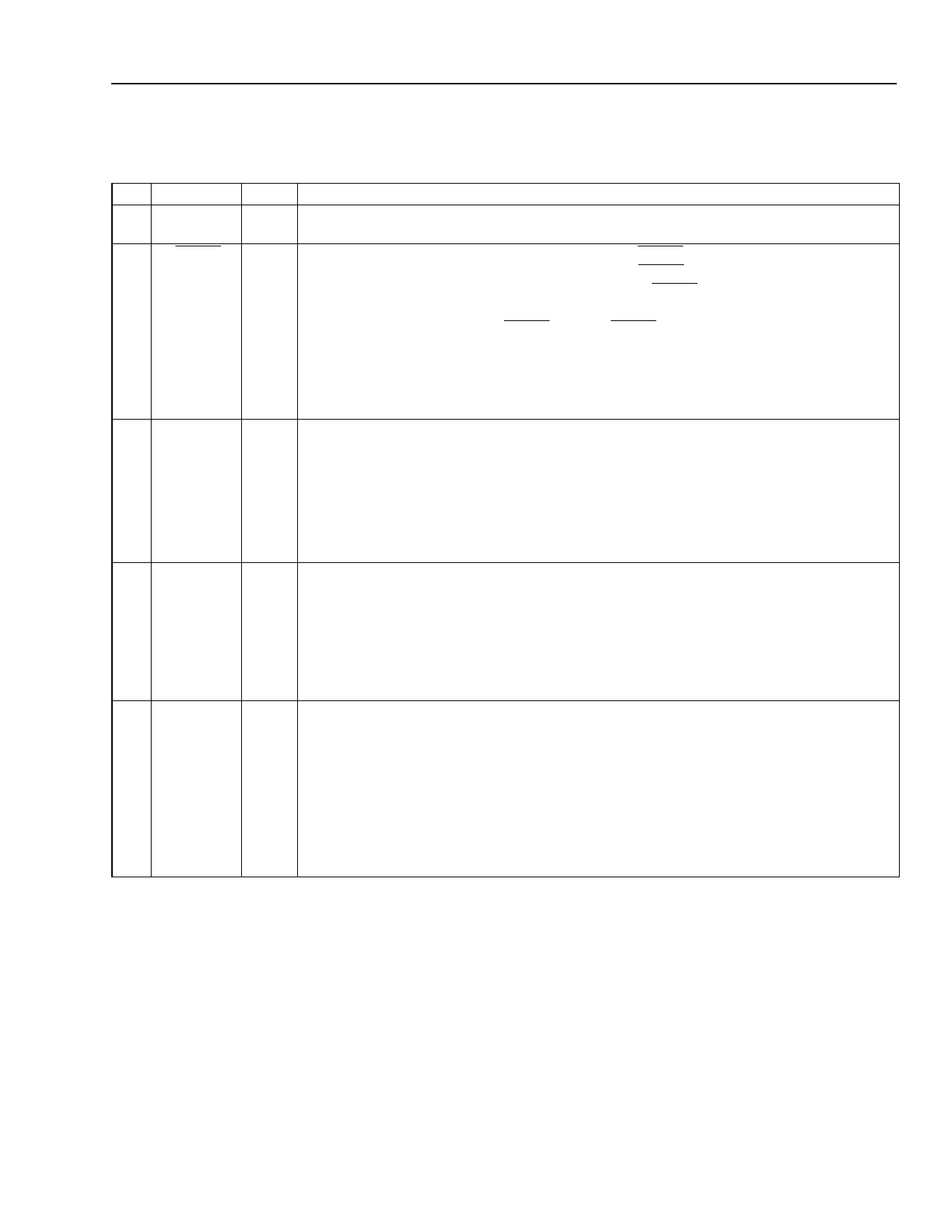
Pin Information (continued)
Table 1. Pin Descriptions (continued)
Pin Symbol Type*
Name/Function
5,
VDDD
13
— Digital Power. 5 V ± 5% power supply pins for digital circuitry.
6 ILOSS
Iu Insertion Loss Test Control (Active-Low). The ILOSS pin is used to control SN1 tone
transmission for maintenance. The OPTOIN and ILOSS pins should not be used at the
same time (i.e., OPTOIN should be held high when ILOSS is active). This pin would typ-
ically be used if an external ANSI maintenance decoder is being used, in which case
the decoder output drives the ILOSS pin. The ILOSS pin is ignored, and the functionality
is controlled by the ILOSS bit (register CFR0, bit 0) if AUTOCTL = 0 (register GR0, bit
3). Internal 100 kΩ pull-up resistor on this pin.
0—U transmitter sends SN1 tone continuously.
1—No effect on device operation.
7
FTE/
TDMDI
Iu Fixed/Adaptive Timing Mode Select. If TDMEN = 1 (register GR2, bit 5, default),
selects S/T-interface timing recovery mode:
0—Fixed timing recovery mode.
1—Adaptive timing recovery mode.
TDM Data In. If TDMEN = 0, this pin is the TDM bus 2B+D data input synchronous with
TDMCLK, and the S/T-interface timing mode is controlled via the FT bit (register GR2,
bit 0). An internal 100 kΩ pull-up resistor is on this pin.
8
PS2E/
Id/O Power Status #2. If TDMEN = 1 (register GR2, bit 5, default), this is an input for the
TDMDO
PS2 bit in transmit U-interface data stream. See PS2 bit description (register GR1, bit
1) for PS1 and PS2 message definition. An internal 100 kΩ pull-down resistor is on this
pin.
TDM Data Out. If TDMEN = 0, this pin is the 2.048 MHz TDM bus 2B+D data output
synchronous with TDMCLK, and PS2 is controlled via the PS2 (register GR1, bit 1) mi-
croprocessor register bit.
9
PS1E/
Id/O Power Status #1. If TDMEN = 1 (register GR2, bit 5, default), this is an input for the
TDMCLK
PS1 bit in transmit U-interface data stream. See PS2 bit description (register GR1,
bit 1) for PS1 and PS2 message definition. If PS1E is not driven by an external control
circuit, it must be pulled up externally with a 10 kΩ or less resistor to indicate the pres-
ence of primary power. An internal 100 kΩ pull-down resistor is on this pin.
TDM Clock. If TDMEN = 0, this pin is the 2.048 MHz TDM clock output synchronous
with U-interface (if active) or is free-running, and PS1 is controlled via the PS1 micro-
processor register bit. TDMCLK will be disabled until at least one of bits 2—7 in register
DFR1 is enabled.
* Iu = input with internal pull-up; Id = input with internal pull-down.
Lucent Technologies Inc.
7
Share Link: 