NTE890 Просмотр технического описания (PDF) - NTE Electronics
Номер в каталоге
Компоненты Описание
Список матч
NTE890 Datasheet PDF : 2 Pages
| |||
Electrical Characteristics (Cont’d): (V+ = +15V, TA = +25°C unless otherwise specified)
Parameter
Test Conditions
Min
Typ
Max
Unit
Current Source
Output Current
Change with Voltage
RS = 14kΩ, Pin1, V+ = 0V
Pin1, V+ = 0V to 10V
–
138.7
–
µA
–
1.0
2.5
µA
Off Leakage
Pin1, V+ = 0V
–
1
50
nA
Reference Voltage
Pin2
1.70
1.90
2.08
V
Logic Output VSAT
VSAT
Off Leakage
Pin3, I = 3mA
Pin3, I = 2mA
–
0.15
0.50
V
–
0.10
0.30
V
–
0.1
1.0
µA
Note 2. The voltage applied to comparator input Pin6 and Pin7 should not be allowed to go below
GND by more than 300mV.
Note 3. Pin3 and Pin5 are open–collector outputs. Shorts between these pins and V+ can cause
overheating and eventual destruction.
Note 4. Reference voltage terminal Pin2 is connected to the emitter of an NPN transistor and is held
at approximately 1.9V. This terminal should be protected from accidental shorts to GND or
supply voltages. Permanent damage may occur if current in Pin2 exceeds 5mA.
Note 5. Avoid stray coupling between Pin5 and Pin7 which could cause false triggering. If false trig-
gering is experienced with the precision mode circuits, bypass Pin6 to GND with at least
0.01µF. This is necessary for operation above 10kHz.
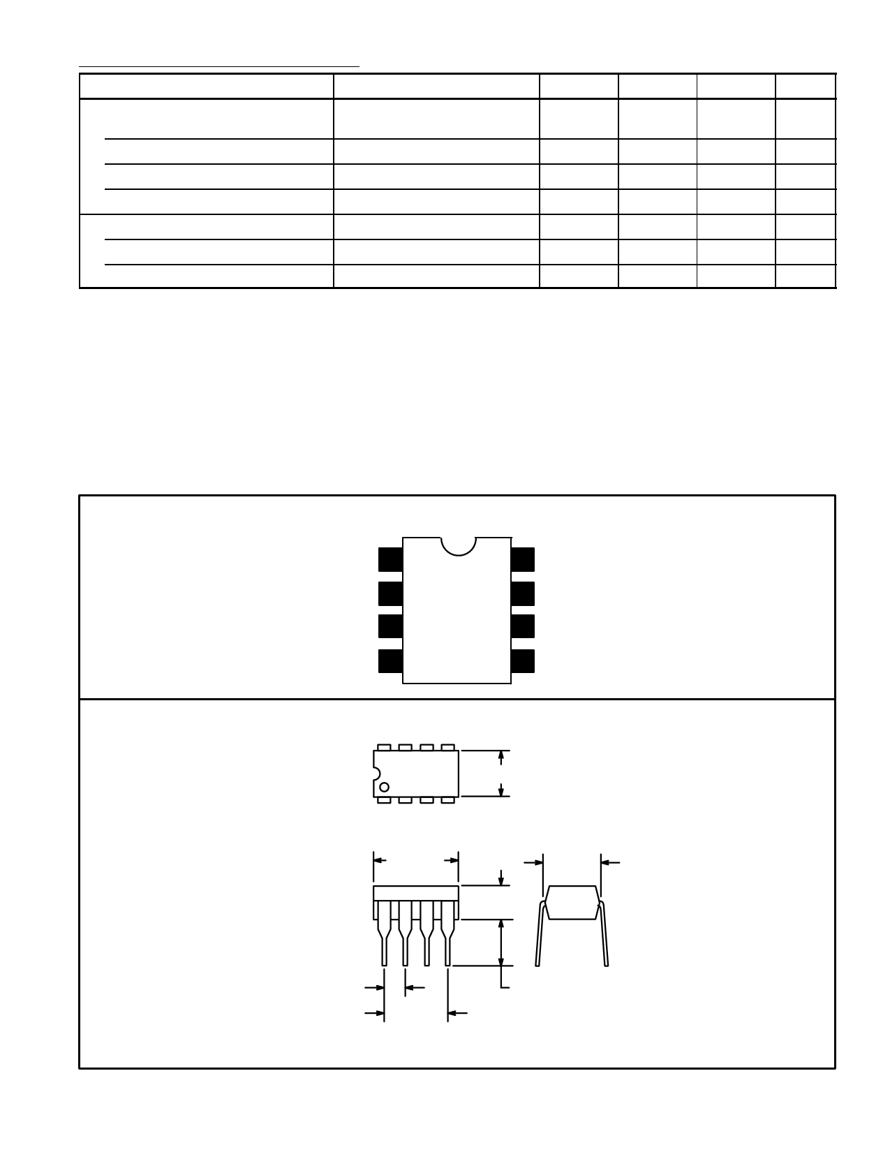
Pin Connection Diagram
Current Source 1
Scale Factor 2
Logic Output 3
GND 4
8 VCC
7 Input Voltage
6 Threshold
5 One–Shot R, C
8
5
.260 (6.6)
1
4
.390 (9.9)
Max
.155
(3.93)
.300
(7.62)
.100 (2.54)
.145 (3.68)
.300 (7.62)
Share Link: 